Qspi flash (hps), Epcq flash, Qspi flash (hps) –50 epcq flash –50 – Altera Arria V SoC Development Board User Manual
Page 58
2–50
Chapter 2: Board Components
Memory
July 2014
Altera Corporation
Reference Manual
QSPI Flash (HPS)
The development board supports one 1-Gb serial NOR flash device for non-volatile
storage of the HPS boot code, user data, and program. The device connects to the HPS
dedicated interface and may contain a secondary boot code.
This 4-bit data memory interface can sustain burst read operations at up to 108 MHz
for a throughput of 54 MBps. Erase capability is at 4 KB, 64 KB, and 32 MB.
lists the QSPI flash pin assignments, signal names, and functions. The
signal names and types are relative to the Arria V SoC in terms of I/O setting and
direction.
EPCQ Flash
The development board supports one 256-Mb serial/quad-serial NOR flash device for
non-volatile storage of the FPGA configuration image. The device connects to the
FPGA dedicated interface through the IDTQS3861 device.
lists the EPCQ flash pin assignments, signal names, and functions. The
signal names and types are relative to the MAX V CPLD 5M2210 System Controller in
terms of I/O setting and direction. Some pins are used in other interfaces as well due
to functionality sharing.
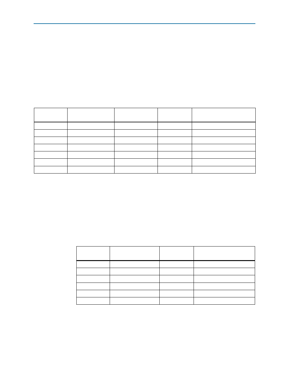
Table 2–29. QSPI Flash Schematic Signal Names and Functions
Board
Reference (U19)
Schematic
Signal Name
Arria V SoC Pin
Number
I/O Standard
Description
16
QSPI_CLK
F15
3.3-V Clock
15
QSPI_IO0
D15
3.3-V Data
bus
8
QSPI_IO1
G15
3.3-V Data
bus
9
QSPI_IO2
M15
3.3-V Data
bus
1
QSPI_IO3
H15
3.3-V Data
bus
7
QSPI_SS0
N15
3.3-V Chip
enable
3
MAX_QSPI_RSTN
—
3.3-V Reset
Table 2–30. EPCQ Flash Schematic Signal Names and Functions
Board
Reference (U28)
Schematic Signal Name
I/O Standard
Description
16
FPGA_DCLK
3.3-V Clock
15
FPGA_AS_DATA0
3.3-V Data
bus
8
FPGA_AS_DATA1
3.3-V Data
bus
9
FPGA_AS_DATA2
3.3-V Data
bus
1
FPGA_AS_DATA3
3.3-V Data
bus
7
FPGA_NCS0
3.3-V Chip
enable