Components and interfaces, Pci express, Components and interfaces –23 – Altera Arria V SoC Development Board User Manual
Page 31: Pci express –23
Chapter 2: Board Components
2–23
Components and Interfaces
July 2014
Altera Corporation
Reference Manual
Components and Interfaces
This section describes the development board's communication ports and interface
cards relative to the Arria V SoC device. The development board supports the
following communication ports:
■
PCI Express
■
10/100/1000 Ethernet (HPS)
■
10/100 Ethernet (FPGA)
■
FMC
■
RS-232 UART (HPS)
■
Real-Time clock (HPS)
■
SFP+
■
I
2
C interface
PCI Express
The PCI Express interface on the development board supports auto-negotiating
channel width from ×1 to ×4 with the following connection speeds:
■
Gen1 at 2.5 Gbps/lane for a maximum of 10 Gbps bandwidth
■
Gen2 at 5 Gbps/lane for a maximum of 20 Gbps bandwidth
The PCIE_REFCLK_P/N signal is a 100-MHz differential input that is driven to the
daughter card through the PCI Express edge connector. This signal connects directly
to a Arria V SoC REFCLK input pin pair using DC coupling. The I/O standard is
High-Speed Current Steering Logic (HCSL).
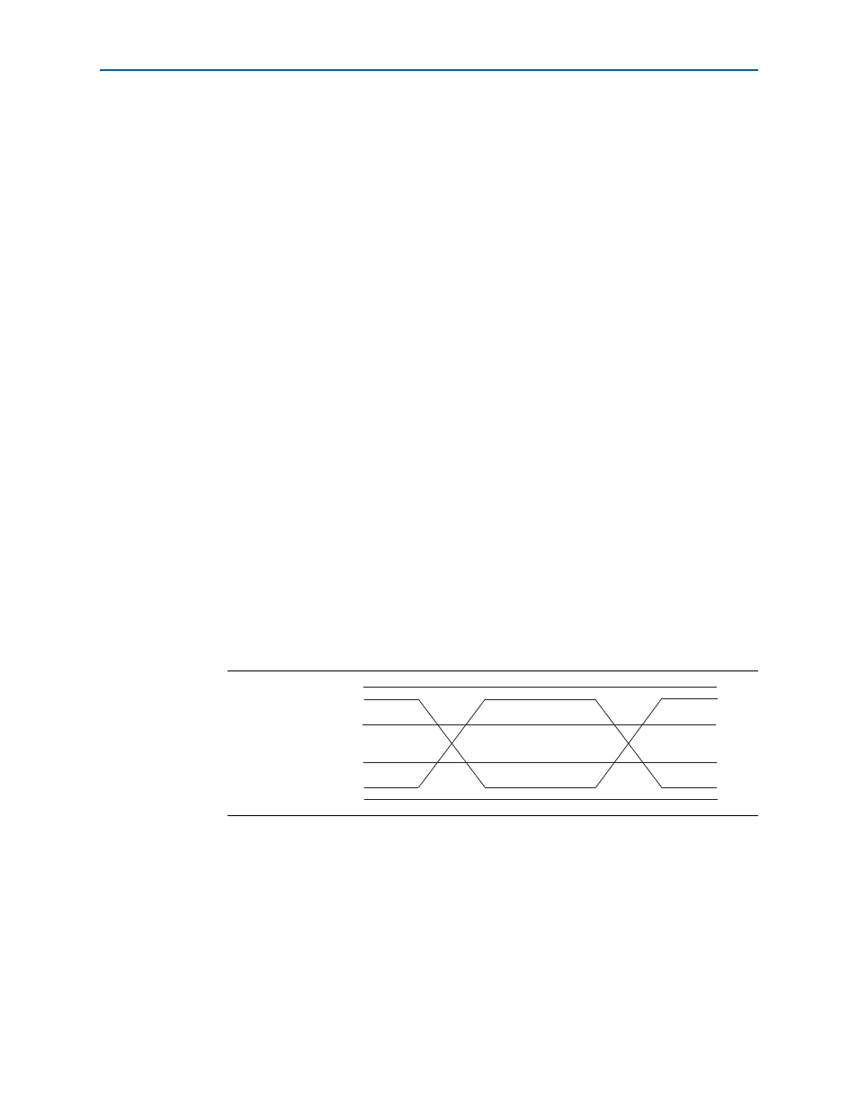
shows the PCI Express reference clock levels.
The PCI Express edge connector also has a presence detect feature for the
motherboard to determine if a card is installed. A jumper is provided to optionally
connect PRSNT1n to any of the three PRSNT2n pins found within the x4 connector
definition. This is to address issues on some PC systems that would base the
link-width capability on the presence detect pins versus a query operation.
summarizes the PCI Express pin assignments. The signal names and
directions are relative to the Arria V SoC.
Figure 2–6. PCI Express Reference Clock Levels
V
MAX
= 1.15 V
V
CROSS MAX
= 550 mV
V
CROSS MIN
= 250 mV
V
MIN
= –0.30 V
REFCLK –
REFCLK +