Ddr3 sdram (hps), Ddr3 sdram (hps) –45 – Altera Arria V SoC Development Board User Manual
Page 53
Chapter 2: Board Components
2–45
Memory
July 2014
Altera Corporation
Reference Manual
DDR3 SDRAM (HPS)
The development board supports three 32Mx16x8 banks DDR3 SDRAM interface
with ECC for very high-speed sequential memory access. The 40-bit data bus
comprises of three ×16 devices with a single address or command bus. This interface
connects to the dedicated HMC for HPS I/O banks on the top edge of the FPGA.
The DDR3 device shipped with this board are running at 533 MHz, for a total
theoretical bandwidth of over 25.6 Gbps. The speed grade of this DDR3 device is
800 MHz with a CAS latency of 9.
lists the DDR3 SDRAM pin assignments, signal names, and functions. The
signal names and types are relative to the Arria V SoC in terms of I/O setting and
direction.
C8
DDR3B_DQ9
AD15
1.5-V SSTL Class I
Data bus
A7
DDR3B_DQ10
AH14
1.5-V SSTL Class I
Data bus
A3
DDR3B_DQ11
AP14
1.5-V SSTL Class I
Data bus
C3
DDR3B_DQ12
AN14
1.5-V SSTL Class I
Data bus
D7
DDR3B_DQ13
AL14
1.5-V SSTL Class I
Data bus
A2
DDR3B_DQ14
AU14
1.5-V SSTL Class I
Data bus
C2
DDR3B_DQ15
AT14
1.5-V SSTL Class I
Data bus
F3
DDR3B_DQS_P0
AH16
Differential 1.5-V
SSTL Class I
Data strobe P byte lane 0
G3
DDR3B_DQS_N0
AG16
Differential 1.5-V
SSTL Class I
Data strobe N byte lane 0
C7
DDR3B_DQS_P1
AF15
Differential 1.5-V
SSTL Class I
Data strobe P byte lane 1
B7
DDR3B_DQS_N1
AE16
Differential 1.5-V
SSTL Class I
Data strobe N byte lane 1
K1
DDR3B_ODT
AD19
1.5-V SSTL Class I
On-die termination enable
J3
DDR3B_RASN
AD17
1.5-V SSTL Class I
Row address select
T2
DDR3B_RESETN
AN15
1.5-V SSTL Class I
Reset
L3
DDR3B_WEN
AP18
1.5-V SSTL Class I
Write enable
L8
DDR3B_ZQ
—
1.5-V SSTL Class I
ZQ impedance calibration
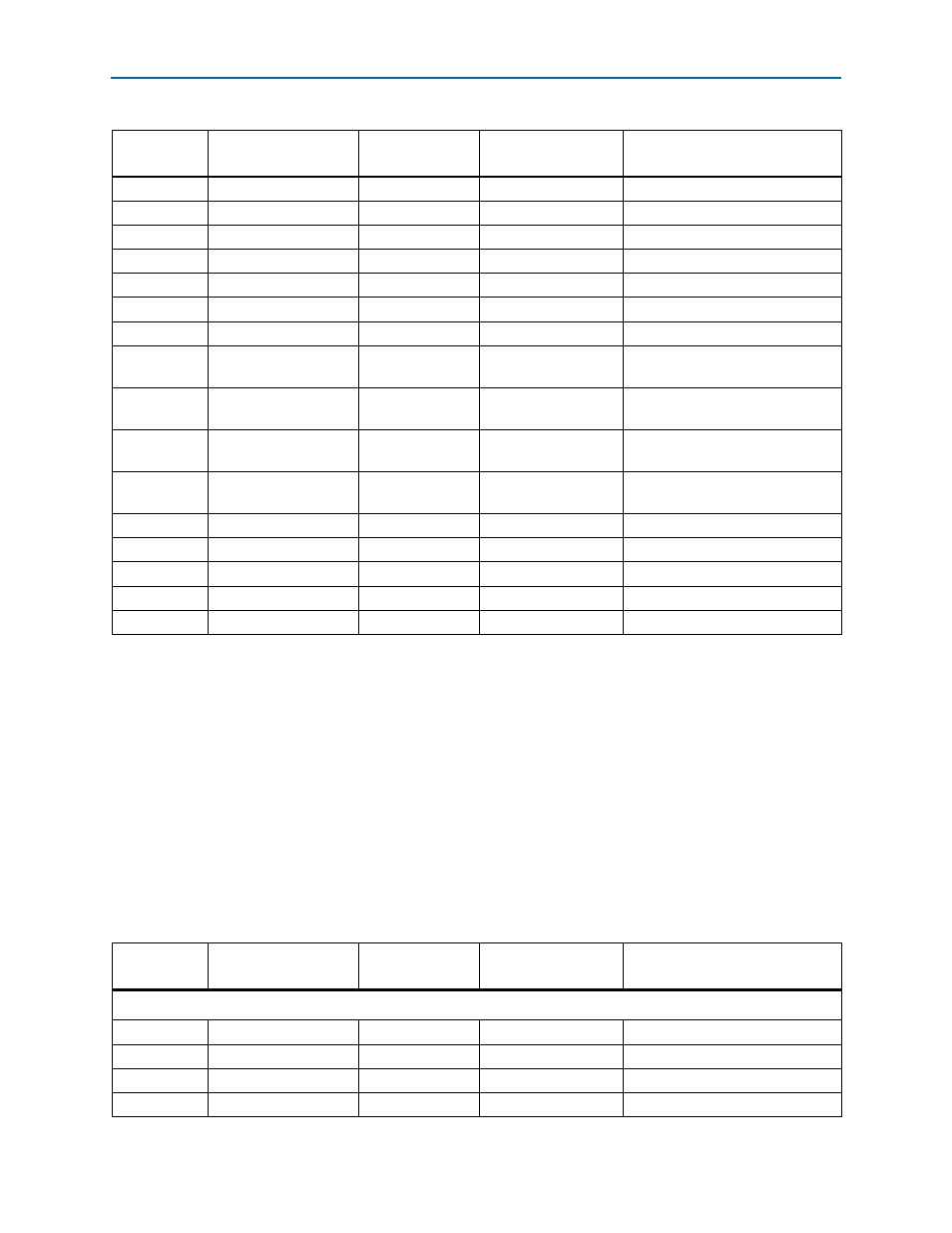
Table 2–27. DDR3 SDRAM Pin Assignments, Schematic Signal Names, and Functions (Part 7 of 7)
Board
Reference
Schematic
Signal Name
Arria V SoC Pin
Number
I/O Standard
Description
Table 2–28. DDR3 SDRAM Pin Assignments, Schematic Signal Names, and Functions (Part 1 of 5)
Board
Reference
Schematic
Signal Name
Arria V SoC Pin
Number
I/O Standard
Description
DDR3 x16 (U51)
N3
DDR3_HPS_A0
N9
1.5-V SSTL Class I
Address bus
P7
DDR3_HPS_A1
M9
1.5-V SSTL Class I
Address bus
P3
DDR3_HPS_A2
N10
1.5-V SSTL Class I
Address bus
N2
DDR3_HPS_A3
M10
1.5-V SSTL Class I
Address bus