Clock circuitry, Clock circuitry –27 – Altera Nios Development Board User Manual
Page 35
Altera Corporation
1–27
September 2004
Nios Development Board Reference Manual, Stratix Edition
Board Components
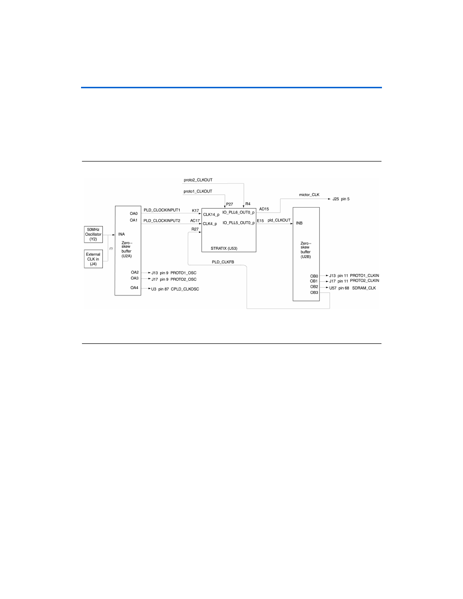
Clock Circuitry
The Nios development board includes a
50 MHz free-running oscillator
and a zero-skew, point-to-point clock distribution network that drives
both the Stratix device and pins on the expansion prototype connectors,
the EPM7128AE device and the Mictor connector. The zero-skew buffer
distributes both the free-running
50 MHz clock and the clock-output from
one of the Stratix's device internal PLLs (CLKLK_OUT1). See
.
Figure 1–21. Clock Circuitry
Note to
(1)
An external clock can be enabled by stuffing location R15 with a 49.9 ohm 0603 resistor and stuffing location R13
with a 330 ohm 0603 resistor.
A socketed 50 MHz free-running oscillator (Y2) supplies the fundamental
operating frequency, and a clock buffer (U2) drives zero-skew clock
signals to various points on the board.
The Stratix device can synthesize a new clock signal internally using on-
chip PLLs, and distribute the clock to various locations on the board by
outputting the clock signal to the IO_PLL5_OUT0_p pin. The clock buffer
drives this signal to the following locations:
■
The PROTO1_CLKIN and PROTO2_CLKIN pins on the expansion
prototype connectors, allowing a user-defined clock to drive each of
the expansion prototype headers.
■
The clock input for the SDRAM memory (U57), allowing SDRAM to
run at a different rate than the clock oscillator.
■
The CLK2_p clock input on the Stratix device. This clock feedback to
the Stratix device is not used by Altera-supplied reference designs,
but is available to the user if necessary.