Chapter 3 – DFI HM961-HM86 User Manual
Page 23
www.dfi .com
Chapter 3 Hardware Installation
23
Chapter 3
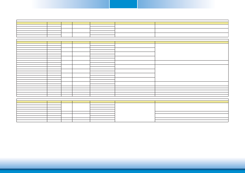
Signal
Pin#
Pin Type
Pwr Rail /Tolerance
HM961-QM87/HM86
Carrier Board
Description
ȟ
ȟ
ȟ
ȟ
USB Signals Descriptions
USB_SSRX2+
C10
USB_SSRX2-
C9
USB_SSTX3+
D13
AC Coupling capacitor
USB_SSTX3-
D12
AC Coupling capacitor
USB_SSRX3+
C13
USB_SSRX3-
C12
Signal
Pin#
Pin Type
Pwr Rail /Tolerance
HM961-QM87/HM86
Carrier Board
Description
LVDS_A0+
A71
LVDS_A0-
A72
LVDS_A1+
A73
LVDS_A1-
A74
LVDS_A2+
A75
LVDS_A2-
A76
LVDS_A3+
A78
LVDS_A3-
A79
LVDS_A_CK+
A81
LVDS_A_CK-
A82
LVDS_B0+
B71
LVDS_B0-
B72
LVDS_B1+
B73
LVDS_B1-
B74
LVDS_B2+
B75
LVDS_B2-
B76
LVDS_B3+
B77
LVDS_B3-
B78
LVDS_B_CK+
B81
LVDS_B_CK-
B82
LVDS_VDD_EN
A77
O CMOS
3.3V / 3.3V
Connect to enable control of LVDS panel power
LVDS panel power enable
LVDS_BKLT_EN
B79
O CMOS
3.3V / 3.3V
Connect to enable control of LVDS panel backlight
LVDS panel backlight enable
LVDS_BKLT_CTRL
B83
O CMOS
3.3V / 3.3V
Connect to brightness control of LVDS panel backlight LVDS panel backlight brightness control
LVDS_I2C_CK
A83
I/O OD CMOS 3.3V / 3.3V
PU 4.7K TO 3V3
Connect to DDC clock of LVDS panel
I2C clock output for LVDS display use
LVDS_I2C_DAT
A84
I/O OD CMOS 3.3V / 3.3V
PU 4.7K TO 3V3
Connect to DDC data of LVDS panel
I2C data line for LVDS display use
Signal
Pin#
Pin Type
Pwr Rail /Tolerance
HM961-QM87/HM86
Carrier Board
Description
LPC_AD0
B4
LPC_AD1
B5
LPC_AD2
B6
LPC_AD3
B7
LPC_FRAME#
B3
O CMOS
3.3V / 3.3V
LPC frame indicates the start of an LPC cycle
LPC_DRQ0#
B8
LPC_DRQ1#
B9
LPC_SERIRQ
A50
I/O CMOS
3.3V / 3.3V
PU 8.2K TO 3V3
LPC serial interrupt
LPC_CLK
B10
O CMOS
3.3V / 3.3V
LPC clock output - 33MHz nominal
ȟ
ȟ
ȟ
ȟ
Connect to LPC device
O LVDS
LVDS
LVDS
Connect to LVDS connector
O LVDS
LVDS
O LVDS
LVDS
Connect to LVDS connector
I CMOS
3.3V / 3.3V
LPC serial DMA request
LVDS Channel B differential clock
LPC Signals Descriptions
O LVDS
LVDS
Connect to LVDS connector
O LVDS
LVDS
Connect to LVDS connector
I/O CMOS
3.3V / 3.3V
LPC multiplexed address, command and data bus
LVDS Channel B differential pairs
O LVDS
LVDS
Connect to LVDS connector
Connect to LVDS connector
LVDS Channel A differential clock
O LVDS
LVDS
Connect to LVDS connector
LVDS Signals Descriptions
O LVDS
LVDS
Connect to LVDS connector
LVDS Channel A differential pairs
O LVDS
Connect to LVDS connector
O LVDS
LVDS
Connect to LVDS connector
I PCIE
AC coupled off Modul
Connect 90ಳ @100MHz Common Choke in series
and ESD suppressors to GND to USB connector
Additional receive signal differential pairs for the SuperSpeed USB data path.
O PCIE
AC coupled on Module
Connect 90ಳ @100MHz Common Choke in series
and ESD suppressors to GND to USB connector
Additional transmit signal differential pairs for the SuperSpeed USB data path.
I PCIE
AC coupled off Modul
Connect 90ಳ @100MHz Common Choke in series
and ESD suppressors to GND to USB connector
Additional receive signal differential pairs for the SuperSpeed USB data path.