Chapter 2 – DFI FS700 User Manual
Page 14
www.dfi .com
Chapter 2 Hardware Installation
14
Chapter 2
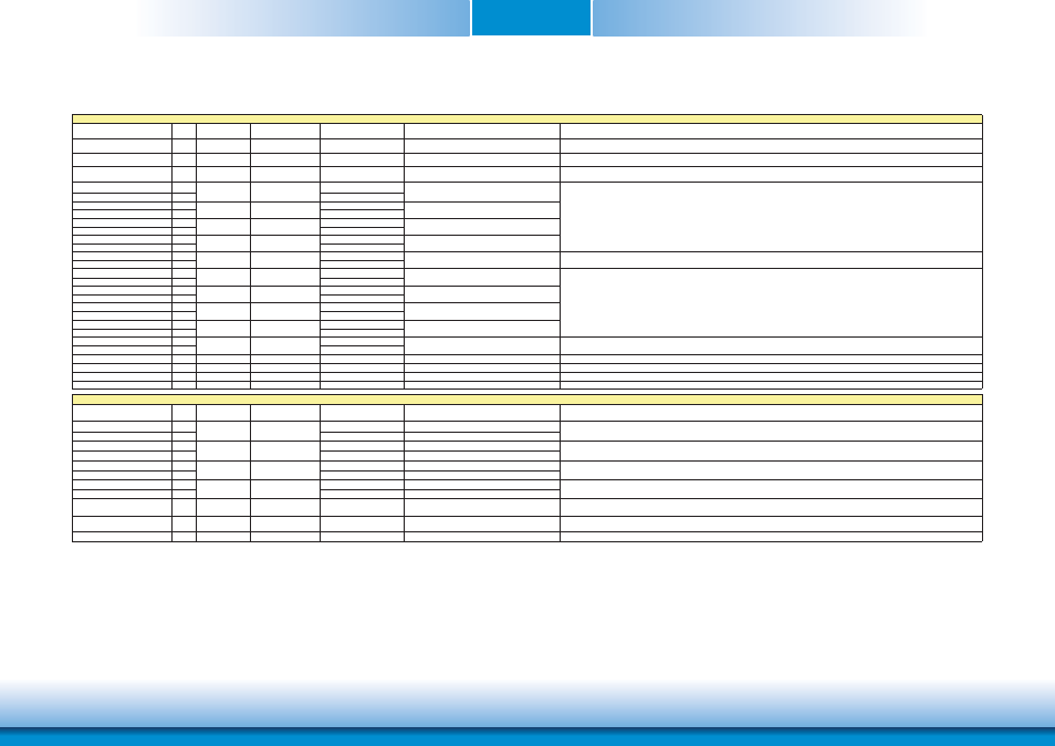
Signal
Pin#
Pin Type
Pwr Rail /Tolerance
DFI-FS700 Series
Carrier Board
Description
LVDS_PPEN
111
O CMOS
3.3V/3.3V
Connect to enable control of LVDS panel power circuit
Controls panel power enable.
LVDS_BLEN
112
O CMOS
3.3V/3.3V
Connect to enable control of LVDS panel backlight powe
circuit.
Controls panel Backlight enable.
LVDS_BLT_CTRL/GP_PWM_OUT0
123
O CMOS
3.3V/3.3V
Connect to brightness control of LVDS panel backlight power
circuit.
Primary functionality is to control the panel backlight brightness via pulse width modulation (PWM).
When not in use for this primary purpose it can be used as General Purpose PWM Output.
LVDS_A0+
99
LVDS_A0-
101
LVDS_A1+
103
LVDS_A1-
105
LVDS_A2+
107
LVDS_A2-
109
LVDS_A3+
113
LVDS_A3-
115
LVDS_A_CLK+
119
LVDS_A_CLK-
121
LVDS_B0+
100
LVDS_B0-
102
LVDS_B1+
104
LVDS_B1-
106
LVDS_B2+
108
LVDS_B2-
110
LVDS_B3+
114
LVDS_B3-
112
LVDS_B_CLK+
120
LVDS_B_CLK-
122
LVDS_DID_CLK/GP_I2C_CLK
127
I/O OD CMOS
3.3V/3.3V
PU 4.7K to 3.3V
Connect to DDC clock of LVDS panel
Primary functionality is DisplayID DDC clock line used for LVDS flat panel detection. If primary functionality is not used it can be as General Purpose I²C bus clock line.
LVDS_DID_DAT/GP_I2C_DAT
125
I/O OD CMOS
3.3V/3.3V
PU 4.7K to 3.3V
Connect to DDC data of LVDS panel
Primary functionality DisplayID DDC data line used for LVDS flat panel detection. If primary functionality is not used it can be as General Purpose I²C bus data line.
LVDS_BLC_CLK
128
I/O OD CMOS
3.3V/3.3V
PU 4.7K to 3.3V
Control clock signal for external SSC clock chip.
LVDS_BLC_DAT
126
I/O OD CMOS
3.3V/3.3V
PU 4.7K to 3.3V
Control data signal for external SSC clock chip.
Signal
Pin#
Pin Type
Pwr Rail /Tolerance
DFI-FS700 Series
Carrier Board
Description
TMDS_CLK-
133
Connect AC Coupling Capacitors 0.1uF to Device
TMDS_CLK+
131
Connect AC Coupling Capacitors 0.1uF to Device
TMDS_LANE0-
145
Connect AC Coupling Capacitors 0.1uF to Device
TMDS_LANE0+
143
Connect AC Coupling Capacitors 0.1uF to Device
TMDS_LANE1-
139
Connect AC Coupling Capacitors 0.1uF to Device
TMDS_LANE1+
137
Connect AC Coupling Capacitors 0.1uF to Device
TMDS_LANE2-
151
Connect AC Coupling Capacitors 0.1uF to Device
TMDS_LANE2+
149
Connect AC Coupling Capacitors 0.1uF to Device
HDMI_CTRL_CLK (SDVO_CTRL_CLK)
152
I/O OD CMOS
3.3V/3.3V
PU 4.7K to 3.3V
DDC based control signal (clock) for HDMI device.
Note: Level shifters must be implemented on the carrier board for this signal in order to be compliant with the HDMI Specification.
HDMI_CTRL_DAT (SDVO_CTRL_DAT)
150
I/O OD CMOS
3.3V/3.3V
PU 4.7K to 3.3V
DDC based control signal (data) for HDMI device.
Note: Level shifters must be implemented on the carrier board for this signal in order to be compliant with the HDMI Specification
HDMI_HPD#
153
I CMOS
3.3V/3.3V
PD 1M and Connect to device Hot Plug Detect
Hot plug detection signal that serves as an interrupt request.
TMDS
O TMDS
TMDS differential pair clock lines.
TMDS differential pair lines lane 0.
TMDS differential pair lines lane 1.
TMDS differential pair lines lane 2.
Connect to LVDS connector
O LVDS
O LVDS
LVDS
LVDS
LVDS
Connect to LVDS connector
Connect to LVDS connector
Connect to LVDS connector
LVDS Flat Panel Signals
O LVDS
LVDS Channel B differential clock
O LVDS
LVDS Channel A differential clock
O LVDS
O LVDS
O LVDS
O LVDS
LVDS
LVDS
LVDS
LVDS
LVDS
LVDS
LVDS
Connect to LVDS connector
Connect to LVDS connector
LVDS Channel A differential pairs
Ther LVDS flat panel differential pairs (LVDS_A[0:3]+/-, LVDS_B[0:3]+/-. LVDS_A_CK+/-,
LVDS_B_CK+/-) shall have 100ƻ terminations across the pairs at the destination. These
terminations may be on the Carrier Board if the Carrier Board implements a LVDS deserializer
on-board
O LVDS
O LVDS
Connect to LVDS connector
Connect to LVDS connector
Connect to LVDS connector
Connect to LVDS connector
LVDS Channel B differential pairs
Ther LVDS flat panel differential pairs (LVDS_A[0:3]+/-, LVDS_B[0:3]+/-. LVDS_A_CK+/-,
LVDS_B_CK+/-) shall have 100ƻ terminations across the pairs at the destination. These
terminations may be on the Carrier Board if the Carrier Board implements a LVDS deserializer
on-board
TMDS
TMDS
TMDS
HDMI Interface Signals
O TMDS
O TMDS
O TMDS