Chapter 2 – DFI FS700 User Manual
Page 16
www.dfi .com
Chapter 2 Hardware Installation
16
Chapter 2
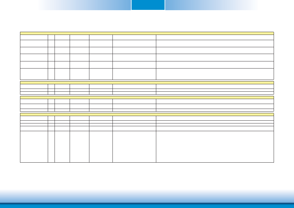
Signal
Pin#
Pin Type
Pwr Rail /Tolerance
DFI-FS700 Series
Carrier Board
Description
MFG_NC0
207
I CMOS
3.3V/3.3V
This pin is reserved for manufacturing and debugging purposes.
May be used as JTAG_TCK signal for boundary scan purposes during production or as a vendor specific control signal. When used as a vendor specific control signal the multiplexer must be
controlled by the MFG_NC4 signal.
MFG_NC1
209
O CMOS
3.3V/3.3V
This pin is reserved for manufacturing and debugging purposes.
May be used as JTAG_TDO signal for boundary scan purposes during production. May also be used, via a multiplexer, as a UART_TX signal to connect a simple UART for firmware and boot loader
implementations. In this case the multiplexer must be controlled by the MFG_NC4 signal.
MFG_NC2
208
I CMOS
3.3V/3.3V
This pin is reserved for manufacturing and debugging purposes.
May be used as JTAG_TDI signal for boundary scan purposes during production. May also be used, via a multiplexer, as a UART_RX signal to connect a simple UART for firmware and boot loader
implementations. In this case the multiplexer must be controlled by the MFG_NC4 signal.
MFG_NC3
210
I CMOS
3.3V/3.3V
This pin is reserved for manufacturing and debugging purposes.
May be used as JTAG_TMS signal for boundary scan purposes during production. May also be used, via a multiplexer, as vendor specific BOOT signal for firmware and boot loader
implementations. In this case the multiplexer must be controlled by the MFG_NC4 signal.
MFG_NC4
204
I CMOS
3.3V/3.3V
This pin is reserved for manufacturing and debugging purposes.
May be used as JTAG_TRST# signal for boundary scan purposes during production. May also be used as control signal for a multiplexer circuit on the module enabling secondary function for
MFG_NC0..3
( JTAG / UART ).
When MFG_NC4 is high active it is being used for JTAG purposes.
When MFG_NC4 is low active it is being used for UART purposes.
Signal
Pin#
Pin Type
Pwr Rail /Tolerance
DFI-FS700 Series
Carrier Board
Description
THRM#
69
I CMOS
3.3V/3.3V
Thermal Alarm active low signal generated by the external hardware to indicate an over temperature situation. This signal can be used to initiate thermal throttling.
THRMTRIP#
71
O CMOS
3.3V/3.3V
Thermal Trip indicates an overheating condition of the processor. If 'THRMTRIP#' goes active the system immediately transitions to the S5 State (Soft Off).
Signal
Pin#
Pin Type
Pwr Rail /Tolerance
DFI-FS700 Series
Carrier Board
Description
FAN_PWMOUT/GP_PWM_OUT1
196
O CMOS
3.3V/3.3V
Primary functionality is fan speed control. Uses the Pulse Width Modulation (PWM) technique to control the Fan's RPM based on the CPU's die temperature.
When not in use for this primary purpose it can be used as General Purpose PWM Output.
FAN_TACHOIN/GP_TIMER_IN
195
I CMOS
3.3V/3.3V
Primary functionality is fan tachometer input. When not in use for this primary purpose it can be used as General Purpose Timer Input.
Signal
Pin#
Pin Type
Pwr Rail /Tolerance
DFI-FS700 Series
Carrier Board
Description
VCC
211-230
Power
Power Supply +5VDC ±5%
VCC_5V_SB
205-206
Power
Standby Power Supply +5VDC ±5%
VCC_RTC
193
Power
3 V backup cell input. VCC_RTC should be connected to a 3V backup cell for RTC operation and storage register non-volatility in the absence of system power.
(VCC_RTC = 2.4 - 3.3 V).
GND
1-2,
23-25,
34,
39-40,
57-58,
73-74,
97-98,
117-118,
135-136,
141-142,
147-148,
159-160,
165-166,
183-184,
197-198,
Power Ground
Power Ground.
Manufacturing Signals
Thermal Management Signals
Fan Control Implementation
Input Power Pins