Fpga, Configuration, Jtag/boundary scan – Sundance SMT387 User Manual
Page 15: Table 1: fpga choices
Version 1.0.3
Page 15 of 42
SMT387 User Manual
FPGA
The module can be fitted with a XC2VP7, XC2VP20, or XC2VP30.
Only flip-chip FF896 package will fit on this board.
The choice of FPGA will be price/performance driven. The following table shows the
main FPGA characteristics.
The choice of the FPGA also determines which board architecture you will get
(amount of logic available, speed, number and type of I/Os, on-board Memory size
and type). For a complete list of the different board architectures, please consult:
Ordering Information
This Xilinx Virtex II Pro, is responsible for the provision of one SHB, 6 Comports, a
PCI interface, 8 RSLs, the global bus and the ZBT memory (In FULL configuration,
see Ordering Information).
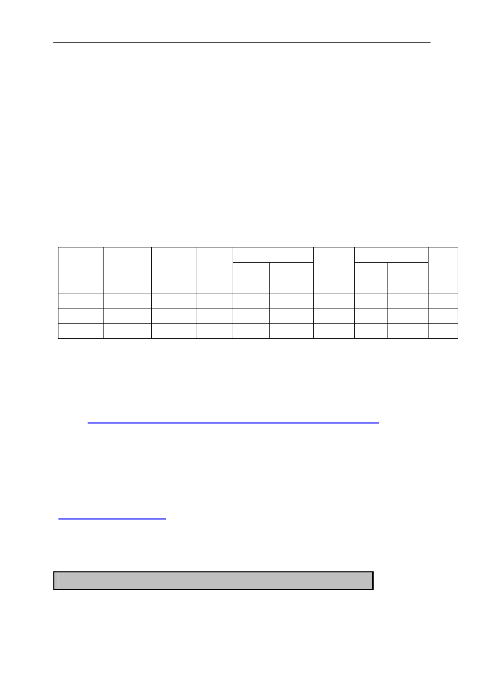
CLB(1 CLB = 4 slices =
Max 128 bits)
SelectRAM Blocks
Device
RocketIO
Transciever
Blocks
PowerPC
Processor
Blocks
Logic
Cells
Slices
Maximum
distributed
RAM Kbits
Multiplier
blocks
18-Kbit
Block
Max RAM
(Kbits)
DCMs
XC2VP7
8 1
11,088
4,928
154
44
44
792
4
XC2VP20
8 2
20,880
9,280
290
88
88
1,584
8
XC2VP30
8 2
30,816
13,696
428
136
136
2,448
8
Table 1: FPGA Choices
Configuration
The FPGA can be configured 2 different ways:
• Using SMT6001 to update the FPGA loaded from flash by the DSP (See
)
• Using the on-board JTAG header and Xilinx JTAG programming tools.
JTAG/Boundary Scan
The JTAG Programmer software is a standard feature of the Alliance Series ™ and
Foundation Series ™ software packages. JTAG Programmer is a part of Web Pack,
which can be downloaded from the following site:
The JTAG chain is composed of the CPLD and the FPGA.
The CPLD is pre-programmed by Sundance.
Do NOT try to reprogram the CPLD without SUNDANCE approval