Chapter 3, Motherboard information – Lanner LEC-3100 User Manual
Page 14
12
Motherboard Information
Chapter 3
Embedded and Industrial Computing
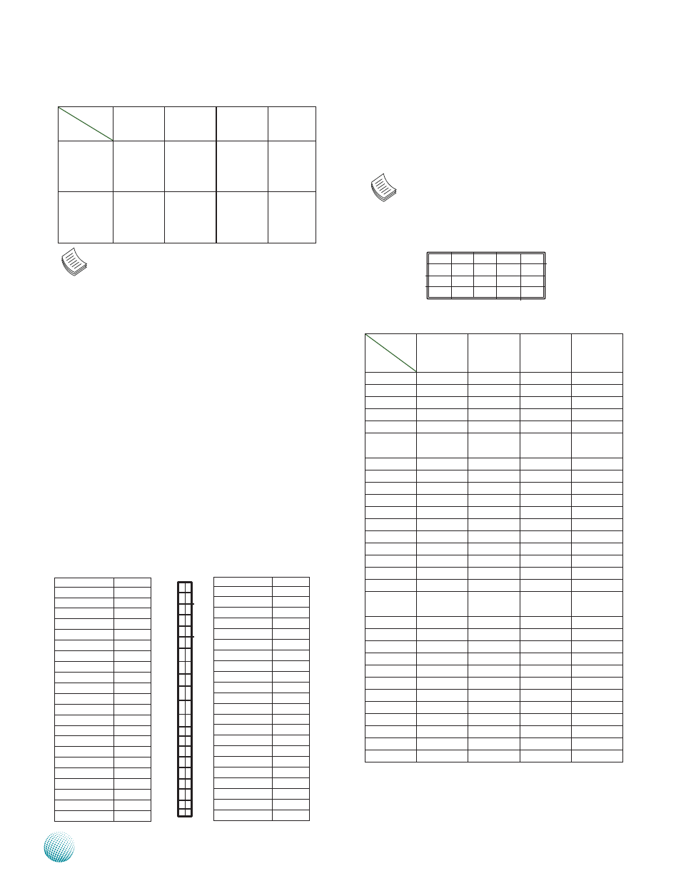
Jumper
Serial Type
SCIT2
SC2T2
SC3T2
SC4T2
RS-422
5-9
6-10
7-11
8-12
3-4
2-3
None
RS-485
5-9
6-10
7-11
8-12
5-6
2-3
None
Note: The RS-485 has automatic flow control by
hardware
COM3~COM 10(CN6 and CN7): The Winbond W83627UHG
Super I/O chipset is connected to the LEC-3100 system
through the LPC bus interfaced to the ICH7M The Super I/O
chipset provides 6 COM ports- two DB-9 male connectors
and 4 by terminal blocks The Fintek F81216AD chipset is
also connected to the system through the LPC bus and
provides the addition of 4 COM ports Together they make
a total of 10 COM ports
IDE Drive Connector (J13): This 2x22 Pin IDE connector
carries the Primary IDE port signals from the ICH7M chipset
This port can be used for connection of two drives (Ultra
ATA 33/66/100 IDE Hard Disks with transferring rate of 33
MB/s, 66 MB/s and 88 9 MB/s respectively are supported )
If two hard disks are connected, one has to be configured
as Master and the other would be Slave, daisy-chained on
a single 44-pin ribbon cable Since the motherboard’s CF
socket (CN4) also connects in parallel to this set of signals,
the CompactFlash can be configured (via jumper J5) to be
either the Master or Slave IDE device
PCI-104 PCI Connector (J11): The mainboard’s PCI-104 PCI
(J11) expansion bus signals are generated by the ICH-7M,
and are essentially identical in function and signaling to a
normal PC motherboard’s PCI bus except for the physical
connector, which is arranged as four 30-pin rows
Note:
We recommend that you use only Lanner
I/O module with this connector to avoid
incompatibility as some pins have been altered
Row NO
Pin NO
Row A
Row B
Row C
Row D
1
KEY2
NC
VCC5
AD0
2
GPIO6
AD2
AD1
VCC5
3
AD5
GND
AD4
AD3
4
C/BE-0
AD7
GND
AD6
5
GND
AD9
AD8
GND
6
AD11
GPIO8
AD10
M66EN_
Pull Low
7
AD14
AD13
GND
AD12
8
VCC3
C/BE-1
AD15
VCC3
9
SERR-
GND
SMB_DAT
PAR
10
GND
PERR-
VCC3
SMB_CLK
11
STOP-
VCC3
LOCK-
GND
12
VCC3
TRDY-
GND
DEVSEL-
13
FRAME-
GND
IRDY-
VCC3
14
GND
AD16
VCC3
C/BE-2
15
AD18
VCC3
AD17
GND
16
AD21
AD20
GND
AD19
17
VCC3
AD23
AD22
VCC3
18
IDSL0_
AD18
GND
IDSL1_
AD19
IDSL2_
AD20
19
AD24
C/BE-3
GPIO9
NC
20
GND
AD26
AD25
GND
21
AD29
VCC5
AD28
AD27
22
VCC5
AD30
GND
AD31
23
REQ-0
GND
REQ-1
GPIO12
24
GND
REQ-2
VCC5
GNT-0
25
GNT-1
GPIO7
GNT-2
GND
26
VCC5
PCICLK0
GND
PCICLK1
27
PCICLK2
VCC5
PCICLK3
GND
28
GND
PIRQ-D
VCC5
PCIRST-
29
NC
PIRQ-A
PIRQ-B
PIRQ-C
30
PCI_PME#
REQ-3
GNT-3
KEY1
44
42
40
38
36
34
32
30
28
26
¦
¦
¦
¦
¦
¦
6
4
2
Function
Pin No.
NC
44
VCC
42
GND
40
HDC CS 1#
38
SA2
36
NC
34
N/C
32
GND
30
GND
28
GND
26
GND
24
GND
22
KEY
20
DATA15
18
DATA14
16
DATA13
14
DATA12
12
DATA11
10
DATA10
8
DATA9
6
DATA8
4
GND
2
43
42
41
39
37
35
33
31
29
27
¦
¦
¦
¦
¦
¦
5
3
1
Function
Pin No.
GND
43
VCC
41
HDD Active
39
HDC CS0#
37
SA0
35
SA1
33
IRQ
31
DMA ACK#
29
IRDY
27
IOR#
25
IOW#
23
DMA REQ#
21
GND
19
DATA0
17
DATA1
15
DATA2
13
DATA3
11
DATA4
9
DATA5
7
DATA6
5
DATA7
3
RESET#
1
D 1
A 1
A 3 0
D 3 0