Chapter 3, Motherboard information – Lanner LEC-3100 User Manual
Page 15
13
Motherboard Information
Chapter 3
Embedded and Industrial Computing
Software Reset Switch by GPIO (SW2): In addition to
the hardware reset switch (SW1), the software reset by
GPIO can be programmed to suit your specific applica-
tion need For example, it could reset a software to its
default settings Refer to the description of CTR on Front
Panel Features in Chapter 1, Introduction Look in your
Driver and Manual CD for sample code to implement this
feature
Hardware Reset Switch(SW1): Compared to SW2, this
is a hardware reset switch which can be used to reset the
system without turning off the power
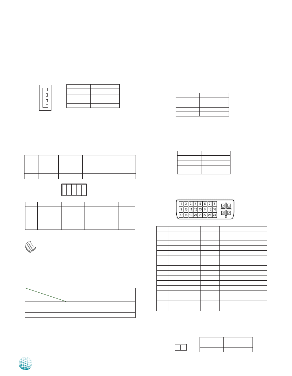
DVI-I Connector (DVII1):
ATX Power Button Connector (PSW1)
USB 2.0 Ports (J8): The board provides 4 USB 2 0 type A
ports Dual ports on the front panel (Reference NO : J7),
one port on the back panel (Reference No : USB2), and
one USB pitch (Reference No : J8) on the board
LCD Module (LCM1): The LCD module connector is a
serial type port which can be connected to display the
real-time operating status and configuration parameters
of the system
Note: In order to connect the LCM, you will need
to adjust BOTH Jumper J4 and J6 accordingly
Note that COM1 will be disabled when the jumper
setting is set to LCD Module use Refer to the COM1
Interface Type and LCM Selection Jumper (J4, J6) on
the previous page for more information
Jumper
Interface Type
J4
J6
Serial Port (Rs-232
/422/485)
1-2
2-3
LCD Module
2-3
1-2
4
3
2
1
USB3
Pin No.
Function
1
USB_VCC
2
USB-
3
USB+
4
GND
1 0 8 6 4 2
9 7 5 3 1
10.
8
6
4
2
Pin No.
KEY Ring Indicator
(RI1#)
Clear to Send
(CTS1#)
Request
to Send
(RTS1#)
Data Set
Ready
(DSR1#)
Function
Ground Data
Terminal
Ready
(DTR1 #)
Transmit Data
(TXD1)
Receive
Data (RXD1)
Data
Carrier
Detect
(DCD1#)
Function
9
7
5
3
1
Pin No.
Pin No.
Function
1
GPIO 12 signal
2
Ground
3
Ground
4
Ground
Pin No.
Function
1
Reset Signal
2
Ground
3
Ground
4
Ground
Pin No.
Function
Pin No.
Function
1
TMDS Data 2¬
13
TMDS Data 3+
2
TMDS Data 2+
14
5V
3
TMDS Data 2/4 shield
15
GND
4
TMDS Data 4¬
16
HOT PLUG DET
5
TMDS Data 4+
17
TMDS Data 0
6
DDC CLOCK
18
TMDS Data 0+
7
DDC DATA
19
TMDS Data 0/5 shield
8
Analog vertical sync
20
TMDS Data 5¬
9
TMDS Data 1¬
21
TMDS Data 5+
10
TMDS Data 1+
22
TMDS CLK shield
11
TMDS Data 1/3 shield
23
TMDS CLK+
12
TMDS Data 3¬
24
TMDS CLK¬
C1
Analog Red
C3
Analog Blue
C2
Analog Green
C4
Analog Horizontal sync
C5
Analog GND
Pin No.
Function
1
PANSW-
2
GND
1 2