Zabg6002 yyww, Zabg 6002 yyww, Part name – Diodes ZABG6002 User Manual
Page 9: Pin 1, Date code, Part name date code year/week
ZABG6002
ZABG6002
Document number: DS32078 Rev. 1 - 2
9 of 12
May 2010
© Diodes Incorporated
A Product Line of
Diodes Incorporated
General Operation
In both modes the R
CAL
1 and R
CAL
2 pins can also be used as logic inputs. If set to a logic high state (>3.0V), the
associated FET bias stages programmed for LNA use (2V drains) are disabled by driving gate pins to -2,5V and
switching drain pins open-circuit. This feature can be used as part of a power management system that turns off
any unwanted stages in a multi input receiver.
The ZABG6002 includes a switched capacitor DC-DC converter that is used to generate the negative supply
required to bias depletion mode FETs used in common source circuit configuration as shown above. This converter
uses two external capacitors, C
NB
the charge transfer capacitor and C
SUB
the output reservoir capacitor. The circuit
provides a regulated -2.5V supply both for gate driver use and for external use if required (for extra discrete bias
stages, mixer bias, local oscillator bias etc.). The -2.5V supply is available from the C
SUB
pin.
If any bias stages are not required, their gate and drain pins may be left open circuit. If all bias stages associated
with an R
CAL
resistor are not required, then this resistor may be omitted.
It must be noted that the exposed pad of the QFN package must be either left floating or connected to Csub.
Ordering Information
Device
Package
Reel size (inches)
Tape width (mm)
Quantity per reel
ZABG6002JB20TC QFN2044
13
12
3,000
ZABG6002Q20TC QSOP20
13
16
2,500
Marking Information
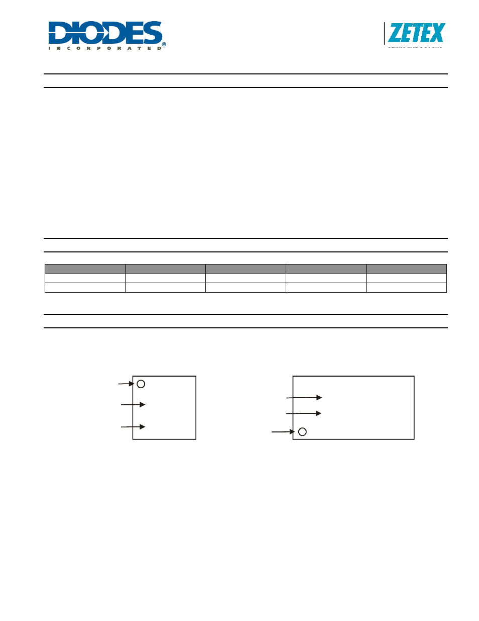
Part Name
Pin 1
ZABG6002
YYWW
Date Code
ZABG
6002
YYWW
Pin 1
Part Name
Date Code
Year/Week
QFN2044
QSOP20