Interface, Interface -3 – Altera Embedded Peripherals IP User Manual
Page 33
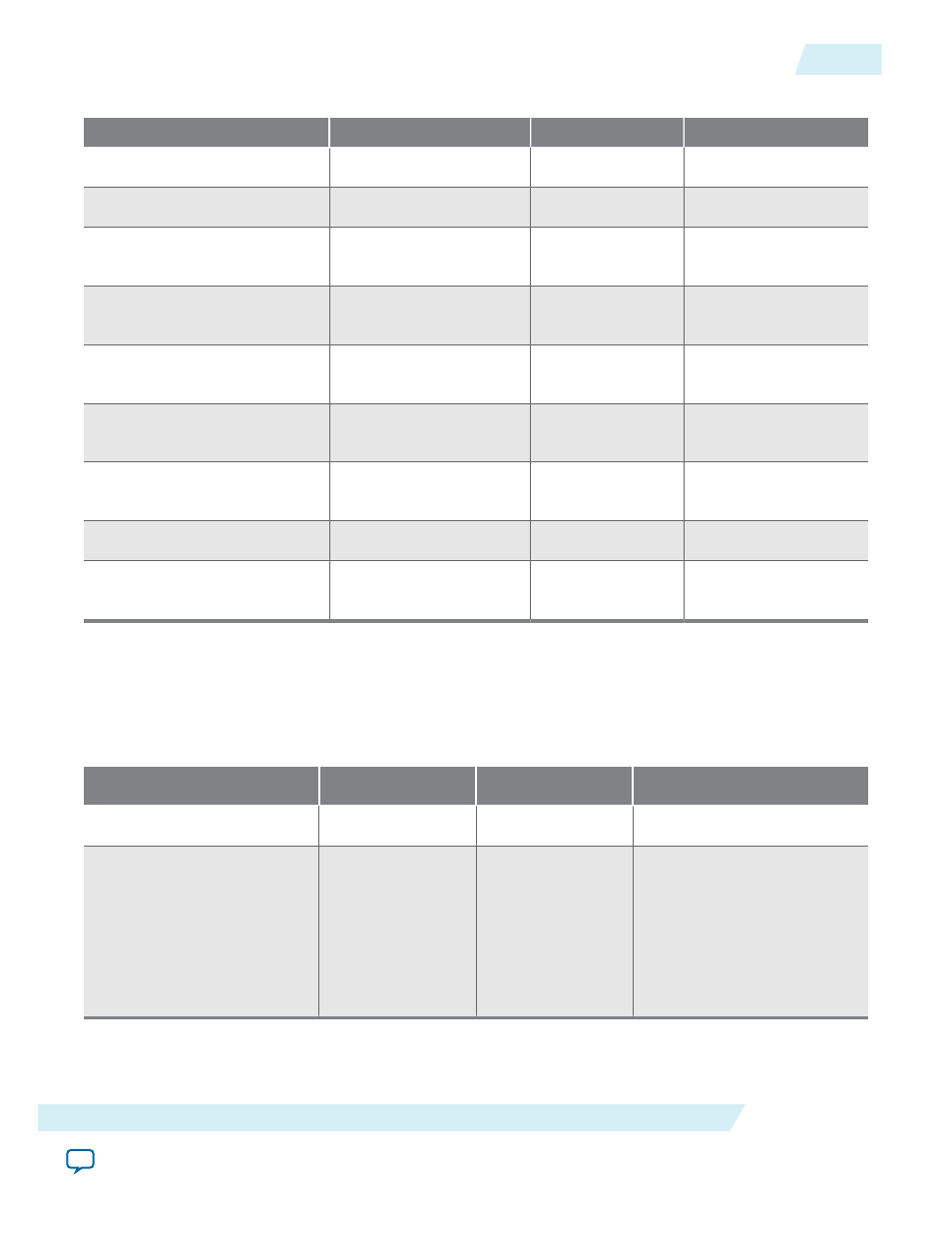
Table 3-2: Configuration Timing Parameters
Parameter
GUI Legal Values
Default Values
Units
CAS latency cycles
1, 2, 3
3
Cycles
Initialization refresh cycles
1:8
2
Cycles
Issue one refresh command
every
0.0:156.25
15.625
us
Delay after power up, before
initialization
0.0:999.0
100.00
us
Duration of refresh command
(
t_rfc
)
0.0:700.0
70.0
ns
Duration of precharge
command (
t_rp
)
0.0:200.0
20.0
ns
ACTIVE to READ or WRITE
delay (
t_rcd
)
0.0:200.0
20.0
ns
Access time (
t_ac
)
0.0:999.0
5.5
ns
Write recovery time (
t_wr
, no
auto precharge)
0.0:140.0
14.0
ns
Interface
The following are top level signals from the SDRAM controller Core
Table 3-3: Clock and Reset Signals
Signal
Width
Direction
Description
clk
1
Input
System Clock
rst_n
1
Input
System asynchronous reset.
The signal is asserted
asynchronously, but is de-
asserted synchronously after
the rising edge of
ssi_clk
.
The synchronization must be
provided external to this
component.
UG-01085
2014.24.07
Interface
3-3
Tri-State SDRAM
Altera Corporation