Altera POS-PHY Level 4 IP Core User Manual
Page 129
Appendix F: Static and Dynamic Phase Alignment
F–5
AC Timing Analysis
December 2014
Altera Corporation
POS-PHY Level 4 IP Core User Guide
1
The calculations follow those in OIF2000.088.4, Appendix D Sample LVDS Timing
Budgets.
f
For timing information on the SPI-4 Phase 2 interface, refer to the Optical
Internetworking Forum (OFI), System Packet Interface Level 4 (SPI-4) Phase 2 Revision 1:
OC-192 System Interface for Physical and Link Layer Devices, OIF-SPI4-02.1, October 2003.
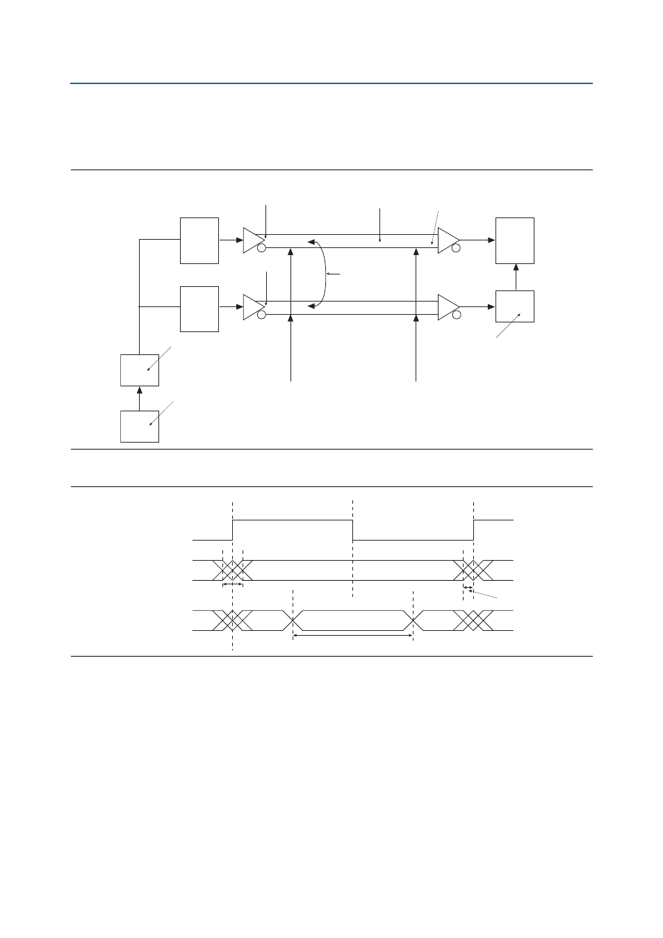
Figure F–3. Timing Analysis Model
Figure F–4. Timing Diagram
Deserializer
PLL
Serializer
for
Data
Channel
Serializer
for
Source
Synchronous
Clock
Clock
Source
Fast
PLL
Clock Source
Jitter
Random (Intrinsic)
Jitter
Buffer Distortion
(Duty Cycle)
Buffer Distortion
(Duty Cycle)
Channel Distortion
Data Dependent Jitter
(Deterministic)
Board Effects
Data Sampling Window
Jitter Attenuation/Pass-Through
plus Intrinsic Jitter
Reference Point A
Reference Point B
Channel-to-Channel
Skew Relative to Clock
Internal Clock
Synchronization
Transmitter
Output Data
Receiver
Input Data
TCCS/2
TCCS
SW
Clock Placement