Altera POS-PHY Level 4 IP Core User Manual
Page 80
5–10
Chapter 5: Functional Description—Transmitter
Clock Structure
POS-PHY Level 4 IP Core User Guide
December 2014
Altera Corporation
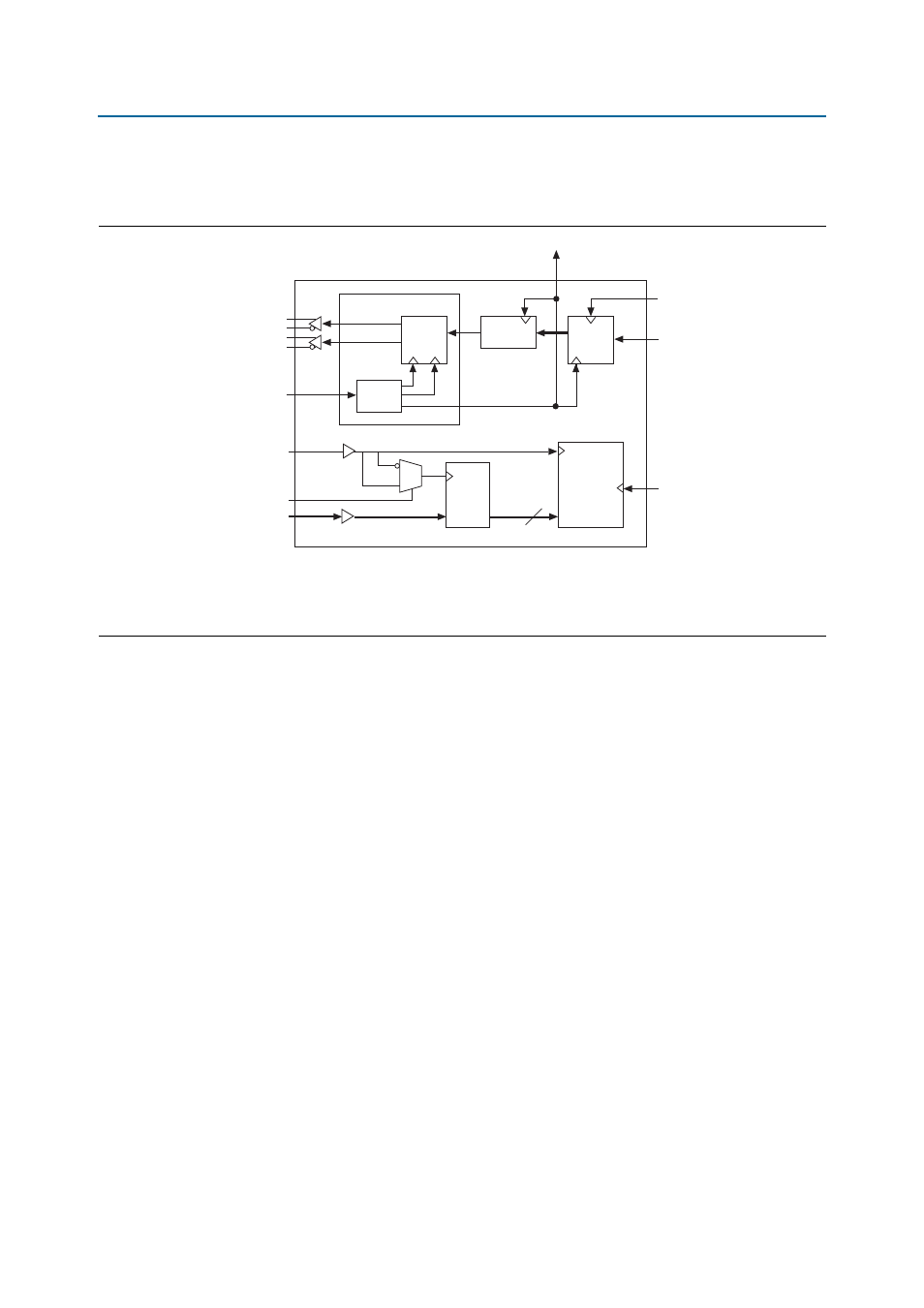
Figure 5–4 on page 5–10
shows the multiple clock domain clocking structure for the
transmitter IP core in full-rate mode.
Figure 5–5 on page 5–11
shows the clocking structure for the transmitter IP core, for
32-bit (quarter rate) SPI-4.2 mode variations. For 32-bit variations, the ALTLVDS_TX
block is replaced by an ALTDDIO_OUT block and there is no LVDS PLL function that
is clocked by trefclk.
Figure 5–4. Clock Layout Diagram (Full Rate)
Notes to
Figure 5–4
:
(1) Stratix and Stratix GX devices use trefclk for tdint_clk. All other device families use the PLL output clock.
(2) The single clock mode removes the separate Atlantic clocks.
(3) The embedded address mode has only one buffer; the individual buffers mode can have more than one buffer.
Data
Processor
SERDES
LVDS
PLL
LVTTL
LVTTL
Status
Processor
Atlantic
Buffer 0
Atlantic
Interface 0
a0_atxclk
tdat[15:0]
tctl
tdclk
txsys_clk
tdint_clk
altlvds Megafunction
tsclk
ctl_ts_statedge
trefclk
tstat[1:0]
2