ABUS Technologies DP Series Smart Pressure Transmitter User Manual
Page 10
ABUS TECHNOLOGIES INC.
M94
10
head or test. The power supply goes to the transmitter through the signal line, with no need of
additional wiring.
In case of the diode being damaged unfortunately, connecting the test terminal can keep
the transmitter working on, except the indicator unable to connect.
No need to shield the signal wire, and litz wire can be used for better effect. Do not lay
together the signal wire and other power wires, to get near to the strong electricity equipment.
The wiring orifice on the housing body of transmitter should be sealed or inserted in a
plug smeared with seal glue to prevent the humidity being accumulated in the housing. In the
case of the wiring not being sealed, the transmitter should be mounted with the wiring orifice
upside down to discharge the moisture.
The signal line may ignore the grounding (hanging) or get to ground at any point on the
loop line. The transmitter housing can have grounding or not, and the power has no need of
being stabilized, even if the power ripples has a peak-to-peak value of 1V. And the output ripples
of transmitter can also be ignored.
Since the transmitter gets grounded by way of capacitance coupling, it is not appropriate
to use a high-voltage mega-ohm meter to check the insulation resistance. The voltage used for
checking the line should be no more than 100 V.
The transmitter circuitry is designed as intrinsic safe circuitry, limiting the output current
below 30 mA DC (35 mA DC under the condition of high temperature or high voltage).
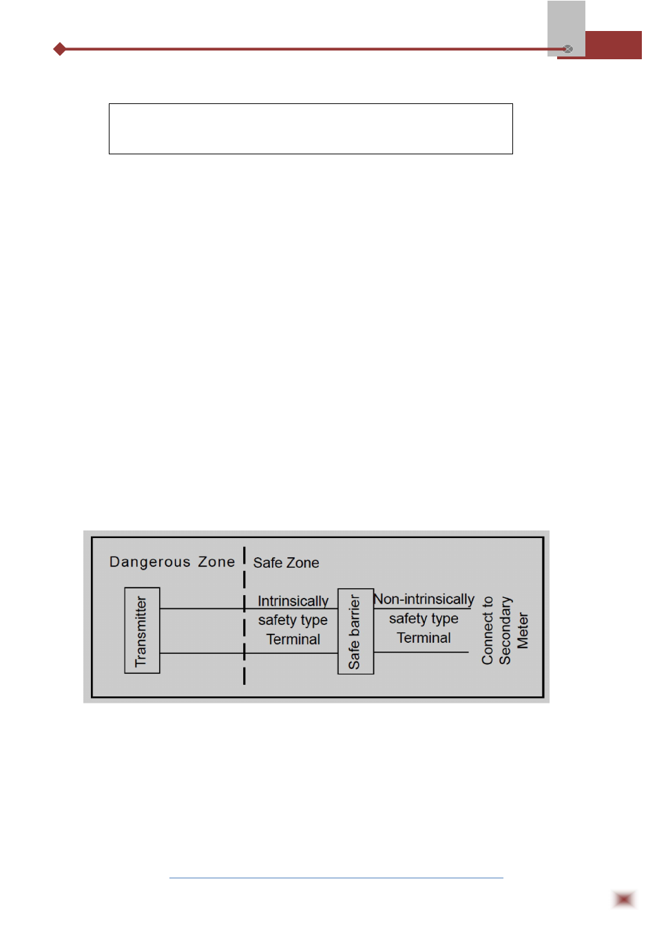
Intrinsically Safety Type Explosion Proof Transmitter System Wiring Diagram
Ui:
28V DC
U
m
≥ 250V AC/DC
li:
30mA
Uo ≤ 28V DC
Pi:
0.84W
lo ≤ 30mA
Po ≤ 0.84W
Note: See GB3836, 4-2000 standard for the definitions of Um, Uo, lo, Po, Ui, li, Pi
The connection wire or cable between safe barrier and transmitter has a largest allowed
distribution capacitance of no more than 0.02µF and the largest allowed distribution inductance
of not more than 2.0mH.
Special Attention:
Do not connect the power signal line to the test terminal; otherwise the
diode inside the test terminal would be destroyed