Table 3-1, P2 signal multiplexing sequence, Functional description – Artesyn MVME7616E Transition Module Installation and Use (April 2015) User Manual
Page 31
Functional Description
MVME7616E Transition Module Installation and Use (6806800A43D)
31
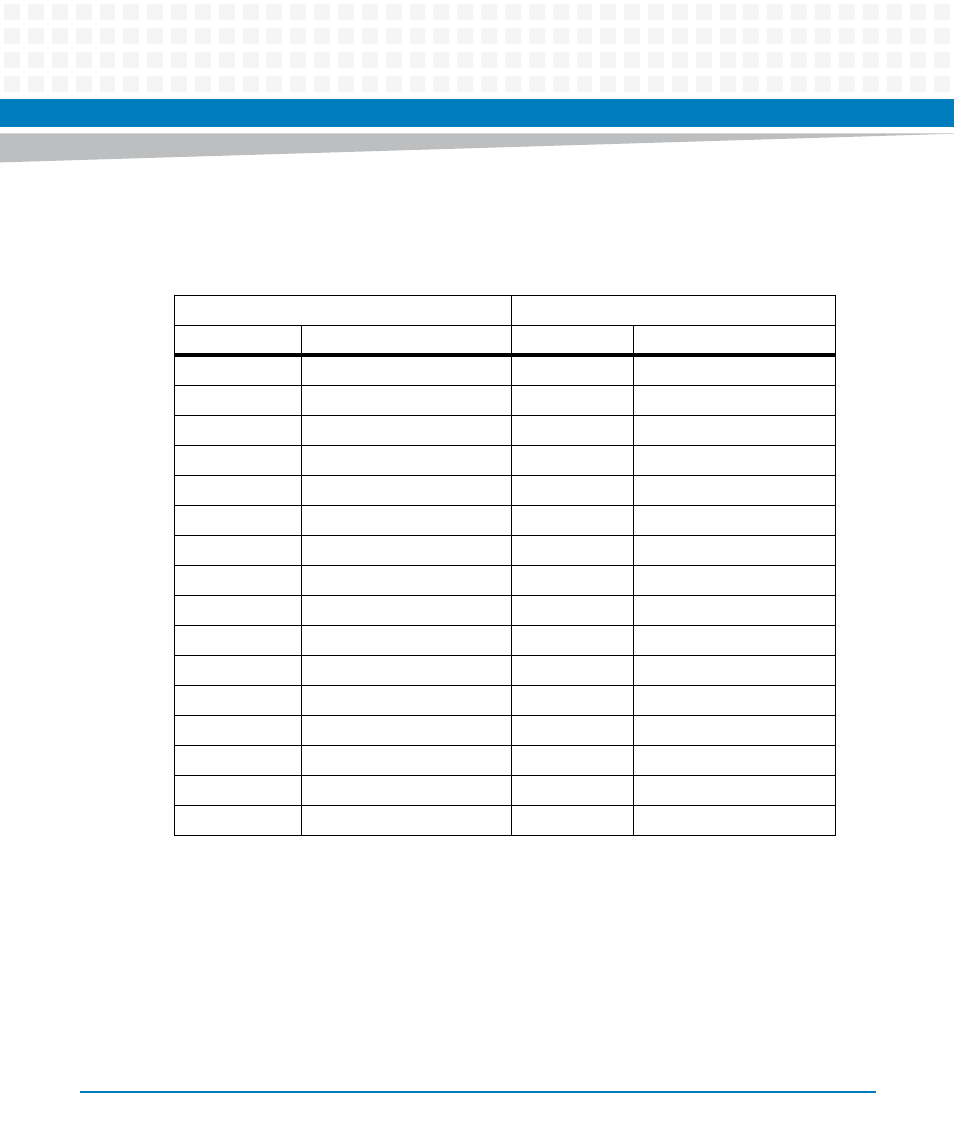
Sixteen time slots are defined and allocated. The signal multiplexing sequences are listed in the
following table.
MXCLK is the 10MHz bit clock for the time-multiplexed data lines, MXDO and MXDI.
MXSYNC# is asserted for one bit time at Time Slot 15 by the MVME5100 and MVME5500
MXSYNC# is used by the MVME761 transition module to synchronize with the VME
modules.
MXDO is the time-multiplexed output line from the main board and MXDI is the time-
multiplexed line from the MVME761 transition module. A 16-to-1 multiplexing scheme is
used with a 10MHz bit rate.
Table 3-1 P2 signal multiplexing sequence
MXDO (from the MVME510x/MVME550x)
MXDI (from the MVME7616E)
Time Slot
Signal Name
Time Slot
Signal Name
0
RTS3
0
CTS3
1
DTR3
1
DSR3/MID1
2
LLB3/MODSEL
2
DCD3
3
RLB3
3
TM3/MID0
4
RTS4
4
RI3
5
DTR4
5
CTS4
6
LLB4
6
DSR4/MID3
7
RLB4
7
DCD4
8
IDREQ#
8
TM4/MID2
9
DTR1
9
RI4
10
DTR2
10
RI1
11
Reserved
11
DSR1
12
Reserved
12
DCD1
13
Reserved
13
RI2
14
Reserved
14
DSR2
15
Reserved
15
DCD2