Power supply, Pinout, Table 6: pinout for different pdi configurations – BECKHOFF FB1111-014x User Manual
Page 12: Figure 2: pdi connector power pin distribution, N table 6, Table 6, Pdi configuration area
Process Data Interfaces
6
FB1111 Piggyback Controller Board
3.2
Power Supply
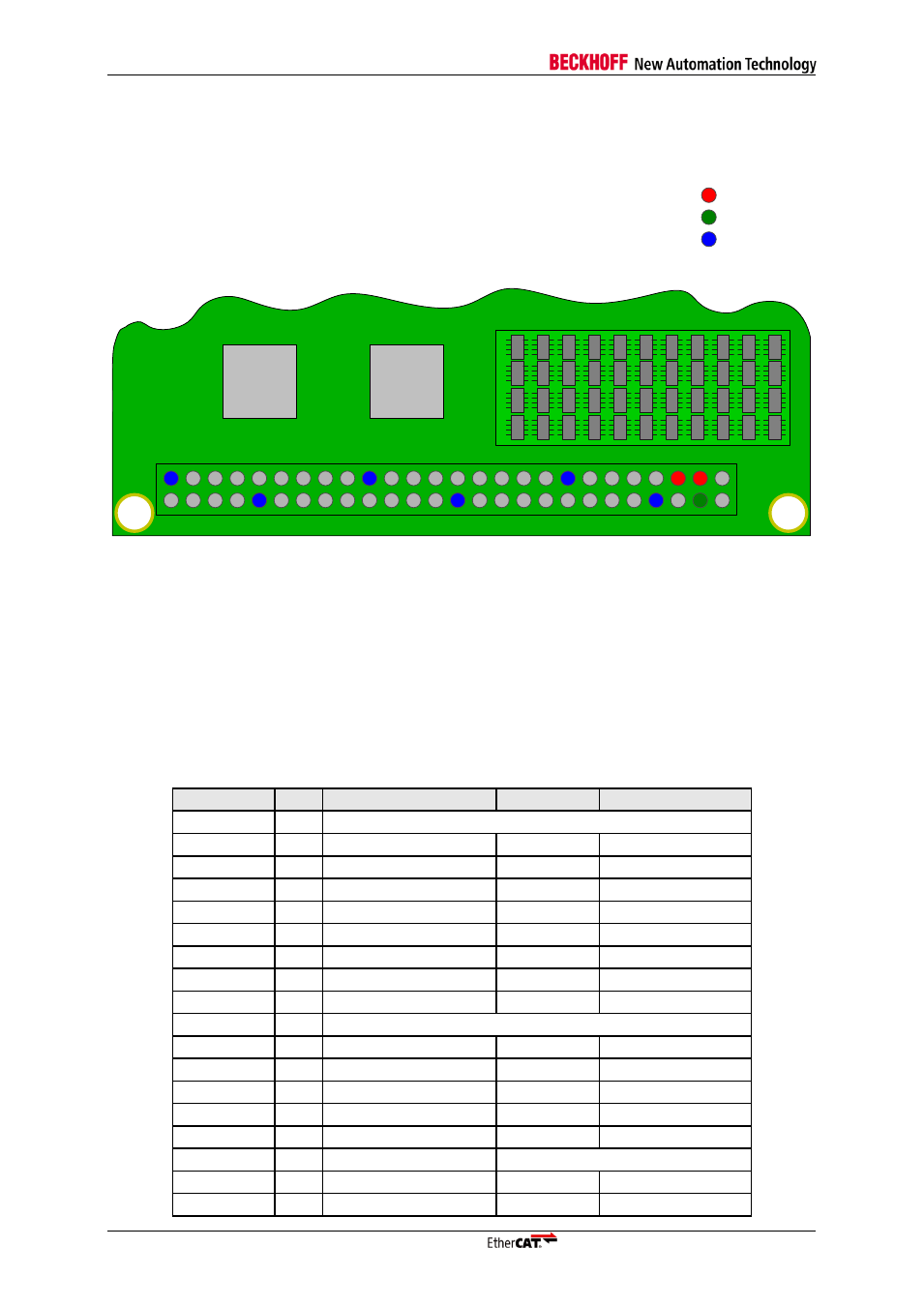
Figure 2 shows the distribution of the power pins on the PDI Connector from top side view.
1
10
19
28
37
46
47 49
50
PHY 1
PHY 0
PDI Configuration Area
VCC (5V)
+3.3V
GND
1
Pin Number
Figure 2: PDI Connector Power Pin Distribution
The Pins 47 and 49 have to be supplied with +5V V
CC.
Pin 50 is a 3.3V Output from one DC-DC con-
verter on the FB1111-014X. The power supply on the FB1111-014X is divided in two sections. One
converter is supplying the PHYs for port 0 and 1. The second DC-DC converter supplies the ET1100
ASIC and all other parts on the printed circuit board. In consequence, the maximum current that can
be driven through the 3.3V output (Pin 50) is limited to 100mA. The GND pins, which are marked blue,
have to be connected to a ground plane on the supplying PCB. All in- and outputs are 3.3V compati-
ble. Applying higher voltages will cause serious damage to the device.
3.3
Pinout
Table 6: Pinout for different PDI Configurations
Pin number Port 0142 - 32bit Digital IO
0141 - SPI
0140 - 16bit as. µC
1
GND
2
PA0
I/O[0]
GPI[6]
A[0]
3
PA1
I/O[1]
GPI[5]
A[1]
4
PA2
I/O[2]
GPI[4]
A[2]
5
PA3
I/O[3]
GPO[7]
A[3]
6
PA4
I/O[4]
GPO[6]
A[4]
7
PA5
I/O[5]
GPO[5]
A[5]
8
PA6
I/O[6]
GPO[4]
A[6]
9
PA7
I/O[7]
GPI[3]
A[7]
10
GND
11
PB0
I/O[8]
GPI[2]
A[8]
12
PB1
I/O[9]
GPI[1]
A[9]
13
PB2
I/O[10]
GPI[0]
A[10]
14
PB3
I/O[11]
GPO[3]
A[11]
15
PB4
I/O[12]
GPO[2]
A[12]
16
PB5
I/O[13]
EEPROM Loaded
17
PB6
I/O[14]
GPO[1]
A[13]
18
PB7
I/O[15]
GPI[11]
CPU_CLK_IN