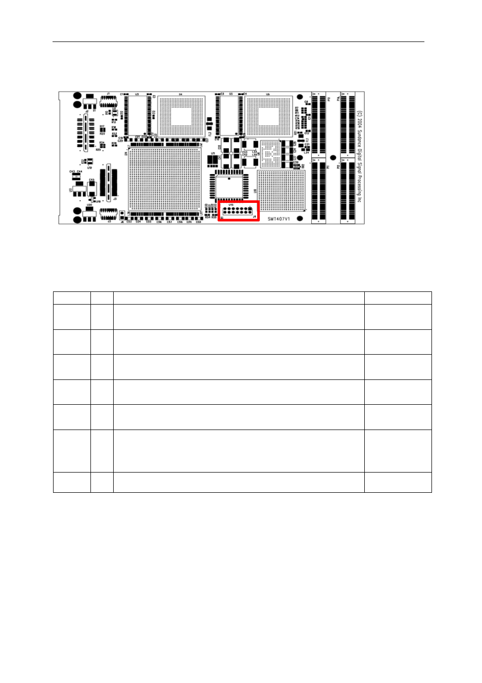
Jtag/multilinx headers, Jtag boundary scan pinout (j4), Figure 12: location of jtag/multilinx header – Sundance SMT407 User Manual
Page 35: Table 9: jtag connector pinout
Version 1.0.0
Page 35 of 38
SMT407 User Manual
JTAG/Multilinx headers
Figure 12: Location of JTAG/Multilinx header
JTAG Boundary scan pinout (J4)
The JTAG/Multilinx header has the following pinout:
Name Pin
Function
Connections
VCC 2
Power.
Supplies VCC (3.3V, 10 mA, typically) to the cable.
To target system
VCC
TMS
4
Test Mode Select.
This signal is decoded by the TAP controller to control test operations.
Connect to system
TMS pin.
TCK 6
Test
Clock.
This clock drives the test logic for all devices on boundary-scan chain.
Connect to system
TCK pin.
TDO 8
Read
Data.
Read back data from the target system is read at this pin.
Connect to system
TDO pin.
TDI
10
Test Data In.
This signal is used to transmit serial test instructions and data.
Connect to system
TDI pin.
GND 1,
3,
5, 7,
9,
11,
13
Ground.
Supplies ground reference to the cable.
To target system
ground
NC 12,
14
No connection
Not connected
Table 9: JTAG Connector pinout