Chapter 3, Board layout – Lanner LVC-5770 User Manual
Page 26
26
Board Layout
Chapter 3
Embedded and Industrial Computing
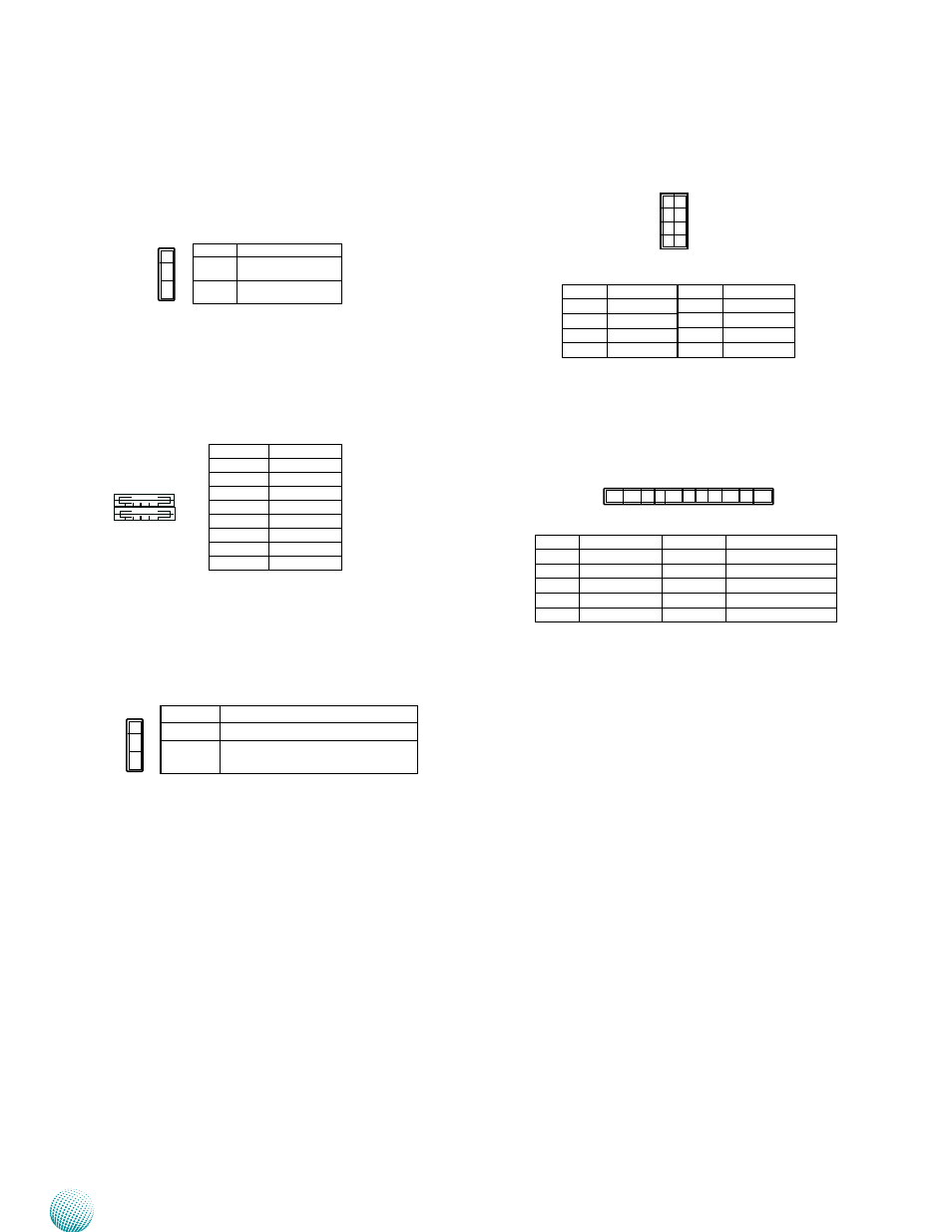
Enable or Disable Daughter Board LEK-IG1 (COMSLT2):
This jumper is for enabling or disabling COM5/COM6 of
daughter board LEK-IG1. If this jumper is set to disable,
the ISM will not work (refer to
Appendix A Using the Ignition
System Manager (ISM)).
Dual USB 2.0 Port Connector #0 and #1 (USB1)
Dual USB 2.0 Port Connector #2 and #3 (USB2)
Dual USB 2.0 Port Connector #4 and #5 (USB3)
Clear CMOS jumper (CMOS1/CMOS2): It is for clearing
the CMOS data. CMOS1clears CMOS data with real-time
clock (RTC) whereas CMOS2 clears CMOS data only.
To erase the CMOS data:
Turn off the computer and unplug the power cord.
Move the jumper cap from pins 1-2 (default) to pins
1.
2-3. Keep the cap on pins 2-3 for about 5-10 seconds,
then move the cap back to pins 1-2.
Plug the power cord and turn on the computer.
2.
Enter BIOS setup to re-enter data.
3.
PS/2 Keyboard and Mouse Connector (KBM1)
Ignition Connector on Board (ignition1): Power
ignition connector.
Pin No.
Pin Name
1-2
Disable
2-3
Enable
1
2
3
1 2 3 4
5 6 7 8
Pin No.
Pin Name
1
VCCUSB
2
USB0N
3
USB0P
4
GND
5
VCCUSB1
6
USB1N
7
USB1P
8
GND
Pin No.
Pin Name
1-2
Normal (Default)
2-3
Clear CMOS and RTC (CMOS1)
Clear CMOS only (CMOS2)
1
2
3
Pin No. Pin Name
1
VCC
3
MDATA
5
KDATA
7
GND
Pin No. Pin Name
2
MCLK
4
NC
6
NC
8
KCLK
1
3
5
7
2
4
6
8
Pin No.
Pin Name
Pin No.
Pin Name
1
DCIN_VCC
6
DC2DC_PWROK
2
DC_VIN
7
COM5_SIN
3
GND
8
SOUT
4
SYS_PWROK
9
PWR_BTN_IGN
5
DC2DC_EN
10
IGNITION
1 2 3 4 10