Altera RAM Initializer User Manual
Page 26
2–14
Confidential—Internal Use Only
Altera Corporation
RAM Initializer (ALTMEM_INIT) Megafunction User Guide
May 2008
Design Example 1: RAM Initialization with Initialization Data File
, the first value, 0x12, is written into the RAM at the fifth
rising edge of the clock, delayed by 4 clock cycles. The subsequent values,
0x23 and 0x24, are written at the eighth and eleventh rising edges of the
clock, respectively. Both writes are delayed by 3 clock cycles. The rest of
the write processes are also delayed by 3 clock cycles each.
Therefore, if your design or application requires an immediate read from
the RAM without waiting for the initialization process to complete, you
can read the first and subsequent values by taking these delays into
consideration. In this design example, for example, you can read the first
value at the sixth clock cycle after the init signal is asserted, which
corresponds to the seventh rising edge of the clock at 42,500 ps. After that,
you can read the subsequent values at intervals of 3 clock cycles.
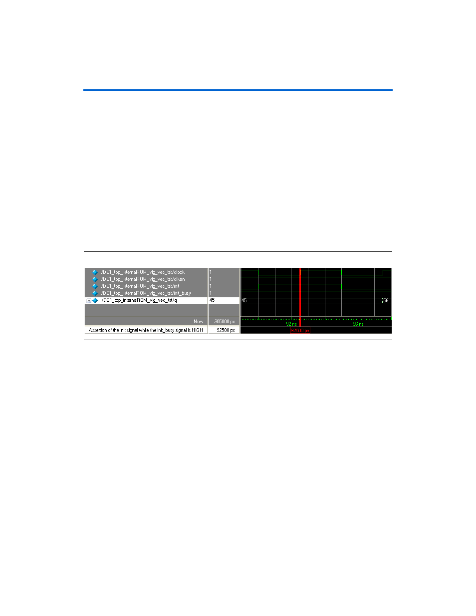
shows the assertion of the init signal while RAM
initialization is still in progress and the init_busy signal is high.
Figure 2–10. Design Example 1: Assertion of the init Signal While Initialization is Still in Progress
At 92,500 ps, the init_busy signal is high to indicate that the
initialization of the RAM is still in progress. When the init signal is
asserted at this point, the initialization process continues uninterrupted.
Therefore, the assertion of the init signal does not affect the current
initialization process while the init_busy signal is high. The init
signal is asserted only once to begin the initialization; to re-initialize the
RAM, you must wait until the current initialization is complete.