Max ii registers, Max ii registers –5, Tton (pb5). refer to – Altera Arria II GX FPGA User Manual
Page 25: Table 6–1 on
Chapter 6: Board Test System
6–5
Using the Board Test System
July 2010
Altera Corporation
Arria II GX FPGA Development Kit, 6G Edition User Guide
■
MAX II ver
—Indicates the version of MAX II code currently running on the board.
The MAX II code resides in the <install
dir>\kits\arriaIIGX_2agx260_fpga\examples directory. Newer revisions of this
code might be available on the
page of the Altera website.
■
MAC
—Indicates the MAC address of the board.
MAX II Registers
The MAX II registers control allow you to view and change the current MAX II
register values as described in
. Changes to the register values with the GUI
take effect immediately. For example, selecting a new frequency in the OCR1 list
immediately changes the clock frequency on the board.
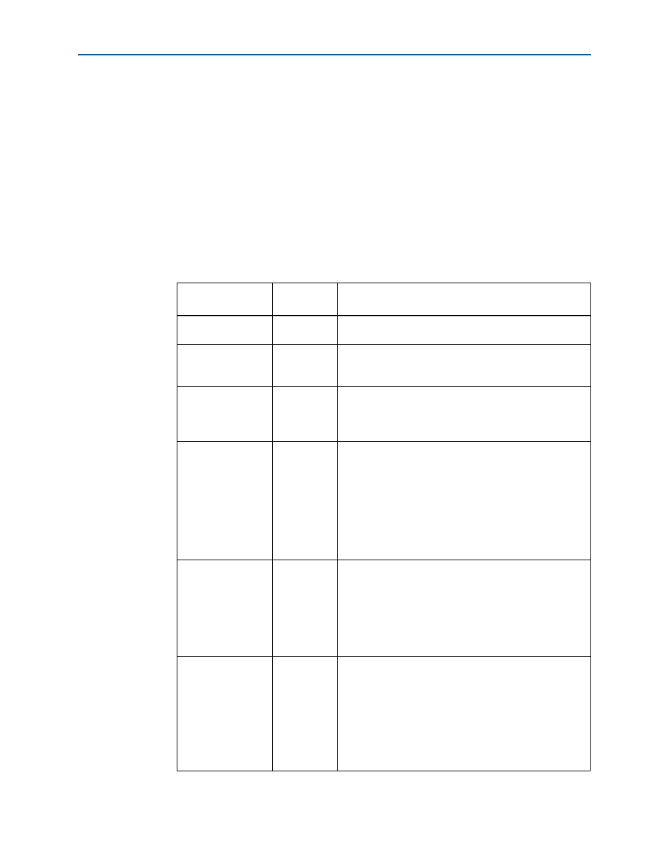
Table 6–1. MAX II Registers
Register Name
Read/Write
Capability
Description
System Reset
(SRST)
Write only
Set to 0 to initiate an FPGA reconfiguration.
Page Select Register
(PSR)
Read / Write
Determines which of the up to eight (0-7) pages of flash
memory to use for FPGA reconfiguration. The flash memory
ships with pages 0 and 1 preconfigured.
Page Select Override
(PSO)
Read / Write
When set to 0, the value in PSR determines the page of
flash memory to use for FPGA reconfiguration. When set to
1, the value in PSS determines the page of flash memory to
use for FPGA reconfiguration.
Page Select Switch
(PSS)
Read only
Holds the current value of the iluminated CONFIG LED (D11-
D13) based on the following encoding:
■
0 = CONFIG LED (D13)and corresponds to the flash
memory page for the factory hardware design
■
1 = CONFIG LED (D12)and corresponds to the flash
memory page for the user hardware 1 design
■
2 = CONFIG LED (D11)and corresponds to the flash
memory page for the user hardware 2 design
Oscillator Control
Register 1 (OCR1)
Read / Write
Determines the U26 oscillator output frequency based on
the following options:
■
0 = 100 MHz
■
1 = 125 MHz
■
2 = 150 MHz
■
3 = 156.25 MHz
Oscillator Control
Register 2 (OCR2)
Read / Write
Determines the U30 oscillator output frequency based on
the following options:
■
0 = 100 MHz
■
1 = 125 MHz
■
2 = 150 MHz
■
3 = 156.25 MHz
You cannot change OCR2 from the GUI.