A. programming the flash memory device, Introduction, Cfi flash memory map – Altera Arria II GX FPGA User Manual
Page 41: Appendix a. programming the flash memory device
July 2010
Altera Corporation
Arria II GX FPGA Development Kit, 6G Edition User Guide
A. Programming the Flash Memory
Device
Introduction
As you develop your own project using the Altera tools, you can program the flash
memory device so that your own design loads from flash memory into the FPGA on
power up. This appendix describes the preprogrammed contents of the common flash
interface (CFI) flash memory device on the Arria II GX FPGA development board, 6G
edition and the Nios II EDS tools involved with reprogramming the user portions of
the flash memory device.
The Arria II GX FPGA development board, 6G edition ships with the CFI flash device
preprogrammed with a default factory FPGA configuration for running the Board
Update Portal design example and a default user configuration for running the Board
Test System demonstration. There are several other factory software files written to
the CFI flash device to support the Board Update Portal. These software files were
created using the Nios II EDS, just as the hardware design was created using the
Quartus II software.
f
For more information about Altera development tools, refer to the
page of the Altera website.
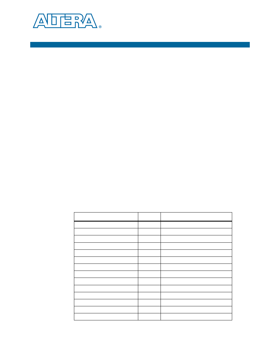
CFI Flash Memory Map
Table A–1
shows the default memory contents of the 512-Mb (64-MB) single-die CFI
flash device. For the Board Update Portal to run correctly and update designs in the
user memory, this memory map must not be altered.
Table A–1. Byte Address Flash Memory Map
Block Description
Size
Address Range
Unused
32 KB
0x03FF8000 - 0x03FFFFFF
Unused
32 KB
0x03FF0000 - 0x03FF7FFF
Unused
32 KB
0x03FE8000 - 0x03FEFFFF
Unused
32 KB
0x03FE0000 - 0x03FE7FFF
User software
16,384 KB
0x0300.0000 - 0x03FDFFFF
Factory software
8,1092 KB
0x02800000 - 0x02FFFFFF
zipfs (html, web content)
8,192 KB
0x02000000 - 0x027FFFFF
User hardware 2
10,880 KB
0x01560000 - 0x01FFFFFF
User hardware 1
10,880 KB
0x00AC0000 - 0x0155FFFF
Factory hardware
10,880 KB
0x00020000 - 0x00ABFFFF
PFL option bits
32 KB
0x00018000 - 0x0001FFFF
Board information
32 KB
0x00010000 - 0x00017FFF
Ethernet option bits
32 KB
0x00008000 - 0x0000FFFF
User design reset vector
32 KB
0x00000000 - 0x00007FFF