Nco ip core timing diagrams, Nco ip core timing diagrams -11, Figure 3-5: single-cycle per output timing diagram – Altera NCO MegaCore Function User Manual
Page 28: Values can change while, Is low
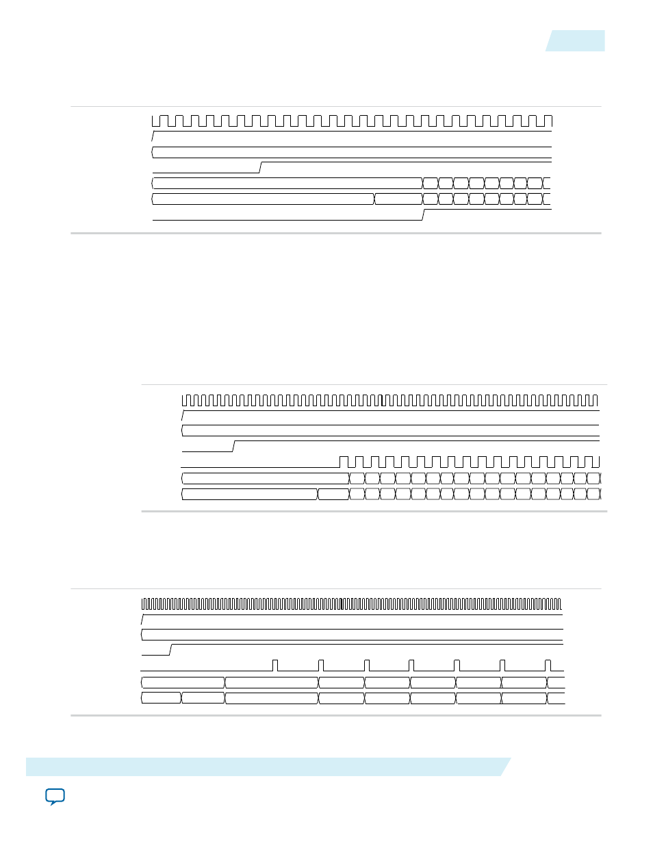
NCO IP Core Timing Diagrams
Figure 3-5: Single-Cycle Per Output Timing Diagram
clk
clken
phi_inc_i
reset_n
fsin_0
fcos_0
out_valid
42949673
0
-3 2057 41... 61.... 8148 10... 12... 13.... 15...
0
32767
32... 32... 32... 32... 31... 31... 30... 29... 28
All NCO architectures, except for serial CORDIC and multi-cycle multiplier-based architectures, output a
sample every clock cycle. After the clock enable is asserted, the oscillator outputs the sinusoidal samples at
a rate of one sample per clock cycle, following an initial latency of L clock cycles. The exact value of L
varies across architectures and parameterizations.
Note: For the non-single-cycle per output architectures, the optional phase and frequency modulation
inputs need to be valid at the same time as the corresponding phase increment value. The values
should be sampled every 2 cycles for the two-cycle multiplier-based architecture and every N cycles
for the serial CORDIC architecture, where N is the magnitude precision.
Figure 3-6: Two-Cycle Multiplier-Based Architecture Timing Diagram
clk
clken
reset_n
fsin_0
fcos_0
out_valid
0
-3 41... 81... 12.... 15... 19... 22... 25...
0
32766
32... 32... 31... 30... 28... 26... 23... 20...
phi_inc_i
85899346
27... 29... 31... 32.... 32... 32... 32...
17... 13... 10... 61.... 20... -2... -6...
31...
-1...
29...
-1...
After the clock enable is asserted, the oscillator outputs the sinusoidal samples at a rate of one sample for
every two clock cycles, following an initial latency of L clock cycles. The exact value of L depends on the
parameters that you set.
Figure 3-7: Serial CORDIC Timing Diagram with N = 8
clk
clken
reset_n
fsin_0
fcos_0
out_valid
0
3
1404
0
2047
phi_inc_i
31457
-2011
2043
1574
257
-1201
1490
-383
129
-1308
-2030
-1657
2046
Note: The
fsin_0
and
fcos_0
values can change while
out_valid
is low.
UG-NCO
2014.12.15
NCO IP Core Timing Diagrams
3-11
NCO IP Core Functional Description
Altera Corporation