Configuring the fpga, Configuring the fpga –3 – Altera Stratix III User Manual
Page 17
Chapter 4: Development Board Setup
4–3
Configuring the FPGA
© August 2008
Altera Corporation
Stratix III Development Kit User Guide
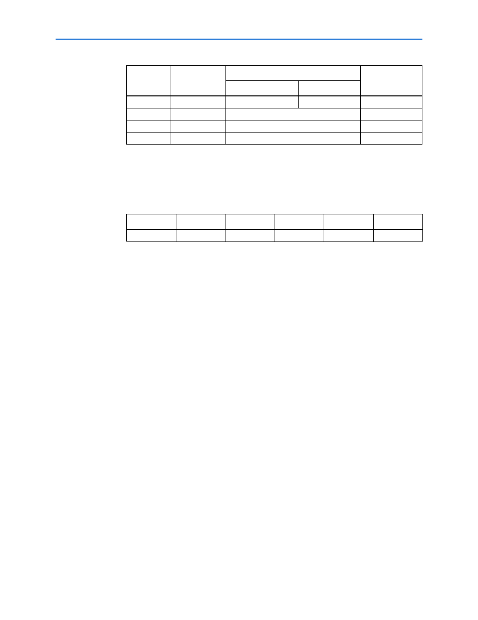
4. Ensure that the 4-position SW1 mini-DIP switches and the two jumpers are set to
the default positions shown in
.
5. Ensure that the J13 MSEL0 GND jumper is ON.
6. Verify that the PGM CONFIG SELECT rotary switch SW3 is set to 0.
At power up, the development board uses a preloaded configuration to demonstrate
that the board is operating correctly.
Power up the development board by performing the following steps:
1. Connect the 16-V DC adapter to the development board and to a power source.
w
Use only the supplied 16-V power supply. Power regulation circuitry on the board
could be damaged by supplies greater than 16 V.
2. Slide the POWER switch to ON. The nearby blue POWER light-emitting diode
(LED) lights up.
3. Confirm that user LEDs 0-7 flash in a scrolling, side-to-side pattern. For
customized configurations, the pattern depends on the application.
f
For information about custom configurations, refer to
Configuring the FPGA
Before configuring the FPGA, ensure that the Quartus II software and the USB-Blaster
driver software are installed on the host computer and the development board is
powered on.
f
For USB-Blaster driver installation information, refer to
.
5
MAX0
PFL Disable
PFL Enable
1
6
MAX1
MAX_DIP1
X
7
MAX2
MAX_DIP2
X
8
MAX3
MAX_DIP3
X
Note to
:
(1) X = don’t care
Table 4–2. Initial Switch and Jumper Settings
DEV_SEL-J2
JTAG_SEL-J3
SW1.1
SW1.2
SW1.3
SW1.4
ON
ON
ON
OFF
OFF
OFF
Table 4–1. Switch SW2 Settings (Part 2 of 2)
Switch
Name
Function
Default
Position
Position 0
Position 1