Featured device: arria v gx fpga, Featured device: arria v gx fpga –6 – Altera Arria V GX FPGA Development Board User Manual
Page 16
2–6
Chapter 2: Board Components
Featured Device: Arria V GX FPGA
Arria V GX FPGA Development Board
November 2013
Altera Corporation
Reference Manual
Featured Device: Arria V GX FPGA
The Arria V GX FPGA development board features two Arria V GX FPGA
5AGXFB3HF40 device (U13 and U16) in a 1517-pin FBGA package.
f
For more information about Arria V device family, refer to the
describes the features of the Arria V GX FPGA 5AGXFB3HF40 device.
lists the Arria V GX FPGA component reference and manufacturing
information.
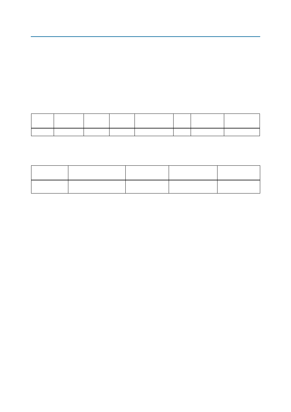
Table 2–2. Arria V GX FPGA Features
ALMs
Equivalent
LEs
M10K RAM
Blocks
Total RAM
Kbits
18-bit × 18-bit
Multipliers
PLLs
Transceivers
Package Type
136,880
362,000
17,260
19,358
2,090
12
24
1517-pin FBGA
Table 2–3. Arria V GX FPGA Component Reference and Manufacturing Information
Board Reference
Description
Manufacturer
Manufacturing
Part Number
Manufacturer
Website
U13, U16
FPGA, Arria V GX F1517,
362K LEs, leadfree
Altera
Corporation
5AGXFB3HF40