I/o resources, I/o resources –7 – Altera Arria V GX FPGA Development Board User Manual
Page 17
Chapter 2: Board Components
2–7
Featured Device: Arria V GX FPGA
November 2013
Altera Corporation
Arria V GX FPGA Development Board
Reference Manual
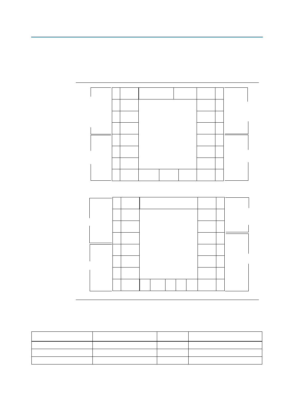
I/O Resources
illustrates the bank organization and I/O count for the Arria V GX FPGA
5AGXFB3HF40 device in the 1517-pin FBGA package.
lists the Arria V GX FPGA 1 pin count and usage by function on the
development board. Clocks are listed under special pins as it uses dedicated I/O pins.
Figure 2–2. Arria V GX FPGA Device I/O Bank Diagrams
Bank 3A
48
Bank 3B
32
Bank 3C
48
Bank 3D
48
Bank 4D
48
Bank 4C
32
Bank 8A
Bank 8B
Bank 8C
Bank 8D
Bank 7D
Bank 7C
48
32
48
48
48
32
Bank 4B
48
Bank 4A
48
Bank 7B
Bank 7A
48
48
GXB_L
XCVRs
GXB_R
XCVRs
PCIe
x8
C2C
x8
A1
AW1
DDR3 x72
1.5 V
USB
2.5 V
Chip-to-Chip
1.8 V
QDRII+
Flash/MAX
ENET
2.5 V
LCD
USER
PCIe
SDI
FMC
HSMA
HSMB
2.5 V
Chip-to-Chip
USER
GXB_R
XCVRs
GXB_L
XCVRs
SFP+
x1
HSMA
x4
C2C
x8
Bank 8A
Bank 8B
Bank 8C
Bank 8D
Bank 7D
Bank 7C
48
32
48
48
48
32
Bank 7B
Bank 7A
48
48
A1
Bank 3A
48
Bank 3B
32
Bank 3C
48
Bank 3D
48
Bank 4D
48
Bank 4C
32
Bank 4B
48
Bank 4A
48
FMC
x4
SDI
x1
SMA
1.5 V
DDR3 x64
HSMB
x4
SFP+
USER
Bullseye
SMA
2.5 V
2.5 V
SMA
5AGXFB3HF40
FPGA 1
5AGXFB3HF40
FPGA 2
Table 2–4. Arria V GX FPGA 1 Pin Count and Usage (Part 1 of 2)
Function
I/O Standard
I/O Count
Special Pins
DDR3 ×72 interface
1.5-V SSTL
125
1 differential ×9 differential DQS
QDRII+ ×36 interface
1.8-V HSTL
103
1 differential ×36 differential DQS
MAX II System Controller
1.8-V CMOS
8
—