Altera Arria V GX FPGA Development Board User Manual
Page 26
2–16
Chapter 2: Board Components
Configuration, Status, and Setup Elements
Arria V GX FPGA Development Board
November 2013
Altera Corporation
Reference Manual
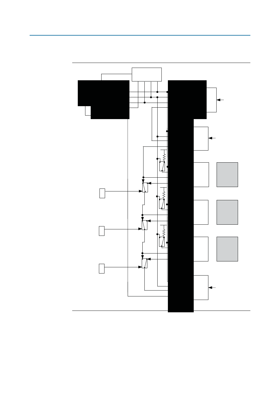
illustrates the JTAG chain.
is located in the JTAG chain DIP switch (SW6) on
the back of the board. To connect a device or interface in the chain, you must set the
corresponding switch from the JTAG chain DIP switch (SW6). The interface in the
JTAG chain depends on the switch settings but the FPGAs and MAX II devices are
always in the JTAG chain.
Figure 2–4. JTAG Chain
TCK
Arria V
(FPGA 1)
FMC Port
HSMC
Port B
Arria V
(FPGA 2)
TMS
TDO
TDI
JTAG Master
DISABLE
JTAG Slave
JTAG Slave
JTAG Slave
JTAG Slave
Analog
Switch
Analog
Switch
ENABLE
ENABLE
ALWAYS
ENABLED
(in-chain)
ALWAYS
ENABLED
(in-chain)
ALWAYS
ENABLED
(in-chain)
DIP switch
DIP switch
JTAG Slave
HSMC
Port A
JTAG Slave
Analog
Switch
ENABLE
2.5V
2.5V
2.5V
Cypress
On-Board
USB-Blaster
II
MAX II CPLD
System
Controller
Installed
FMC
Card
Installed
HSMC
Card
Installed
HSMC
Card
10-pin
JTAG Header