Altera Arria V GX FPGA Development Board User Manual
Page 45
Chapter 2: Board Components
2–35
General User Input/Output
November 2013
Altera Corporation
Arria V GX FPGA Development Board
Reference Manual
f
For more information about the application circuit of the LMH0303SQx cable driver,
refer to the cable driver data sheet at
.
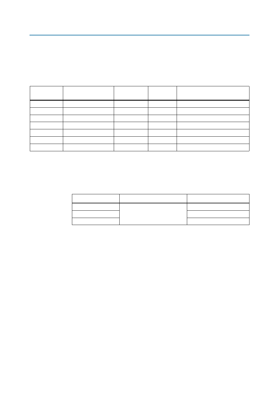
Table 2–37
summarizes the SDI video output interface pin assignments, signal names,
and functions.
The cable equalizer supports operation at 270 Mbit SD, 1.5 Gbit HD, and 3.0 Gbit
dual-link HD modes. Control signals are allowed for bypassing or disabling the
device, as well as a carrier detect or auto-mute signal interface.
Table 2–38
lists the cable equalizer lengths.
Table 2–37. SDI Video Output Interface Pin Assignments, Schematic Signal Names, and Functions
Board
Reference (U24)
Schematic
Signal Name
Arria V GX FPGA
Pin Number
I/O Standard
Description
1
SDI_A_TX_P
AH3
1.4-V PCML
SDI video input P
2
SDI_A_TX_N
AH4
1.4-V PCML
SDI video input N
4
SDI_A_TX_RSET
—
3.3-V
Device reset pull up register
6
SDI_A_TX_EN
AK31
2.5-V
Device enable
10
SDI_A_TX_SD_HDN
M20
2.5-V
High definition select
11
SDI_A_TXDRV_N
—
3.3-V
SDI video output from cable driver N
12
SDI_A_TXDRV_P
—
3.3-V
SDI video output from cable driver P
Table 2–38. SDI Cable Equalizer Lengths
Data Rate (Mbps)
Cable Type
Maximum Cable Length (m)
270
Belden 1694A
400
1485
140
2970
120