Featured device, Featured device –5 – Altera Cyclone III FPGA Starter Board User Manual
Page 13
Altera Corporation
2–5
April 2012
Cyclone III FPGA Starter Board Reference Manual
Board Components and Interfaces
Featured
Device
The Cyclone III FPGA Starter Kit features the EP3C25F324 device (U1) in
a 324-pin FineLine BGA (FBGA) package
.
Table 2–2
lists Cyclone III
device features.
Clock Circuitry
Oscillator
Clock
Y1
50-MHz clock oscillator used for the system
clock.
Power Supply
Input
DC power
jack
J2
12-V DC unregulated power source.
Input
Power switch
SW1
Switches the board’s power on and off.
Probe point
Current sense
resistor
JP6
Measure FPGA core power with current
sense resistor.
N/A
Probe point
Current sense
resistor
JP3
Measure 2.5-V I/O power (shared between
devices) with current sense resistor.
N/A
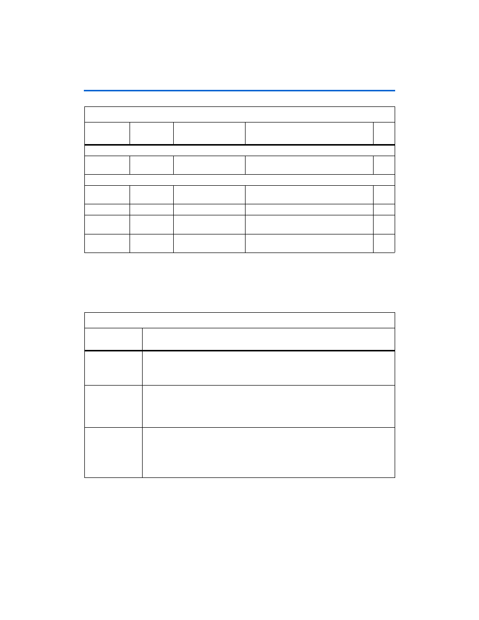
Table 2–1. Cyclone III FPGA Starter Board (Part 2 of 2)
Type
Component/
Interface
Board Reference
Description
Page
Table 2–2. Cyclone III Device Features
Architectural
Feature
Results
Altera’s
third-generation of
low-cost FPGAs
●
Lowest overall FPGA system cost available
●
Staggered I/O ring to decrease die area
●
Wide range of low-cost packages
●
Support for low-cost serial and parallel flash for configuration options
Lowest power
consumption
FPGA available
●
Based on the TSMC’s low-power 65nm process
●
Supports hot-socketing
●
Unused I/O banks can be powered down
●
Extends battery life for portable or hand-held applications
●
Eliminates or reduces cooling system costs
Increased system
integration
●
Densities up to 119,088 logic elements
●
High memory-to-logic ratio
●
Highest multiplier-to-logic ratio in the industry
●
Up to four dynamically reconfigurable, cascadable phase-locked-loops (PLLs), each
with up to five outputs
●
Multi-value on-chip termination (OCT) support with calibration feature.