Jumpers, Jumpers –7 – Altera Cyclone III FPGA Starter Board User Manual
Page 15
Altera Corporation
2–7
April 2012
Cyclone III FPGA Starter Board Reference Manual
Board Components and Interfaces
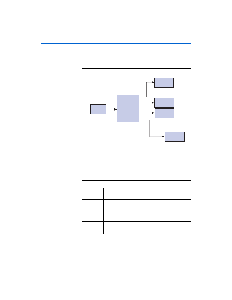
Figure 2–3
shows the simplest clocking scheme with a single clock input;
however, much more complex clocking schemes can be implemented
with Cyclone III FPGAs.
Figure 2–3. Cyclone III FPGA Starter Board’s Clocking Scheme
Jumpers
lists board jumpers and jumper operational descriptions.
50 MHz
Oscillator
16 MB
Parallel Flash
SSRAM
HSMC
Cyclone III
EP3C25F324
B9, V9
32 MB DDR
Note: Reference numbers are FPGA pin numbers.
Out:
A1,
C14,
D14,
V18,
U18
In:
A9
F18,
F17
N18,
N17
U2, V2
A2
H4
Table 2–5. Board Jumpers (Part 1 of 2)
Jumper Board
Reference
Jumper Operational Descriptions
JP1 and JP2
Removing both shunts adds the HSMC connector to the JTAG
chain. If the shunts are in place on both jumpers, then the HSMC
connector is removed from the JTAG chain.
JP3
Sense resistor for measuring the power consumed by the 2.5 V
supply to V
CCIO
,
the DDR, the flash I/O, and the SSRAM.
JP4
1.25 V termination supply for DDR2. To supply an external
voltage, remove the jumper and connect the external supply to
pin 2. (Pin 2 has a rounded shape on the bottom of the board.)