Power supply, Power supply –19 – Altera Cyclone III FPGA Starter Board User Manual
Page 27
Altera Corporation
2–19
April 2012
Cyclone III FPGA Starter Board Reference Manual
Board Components and Interfaces
Power Supply
The power supply block distributes clean power from the 12 V input
supply to the Cyclone III device through on-board regulators.
To provide various voltage options, the board uses several Linear
Technologies’ regulators. Switching regulators are used for digital circuits
and linear regulators are used for analog circuits. Board regulators are
used to generate the voltages listed in
Table 2–17
.
flash_sram_dq25
A18 Bidirectional
2.5
V
19
flash_sram_dq26
F8 Bidirectional
2.5
V
22
flash_sram_dq27
D7 Bidirectional
2.5
V
23
flash_sram_dq28
F6 Bidirectional
2.5
V
24
flash_sram_dq29
E6 Bidirectional
2.5
V
25
flash_sram_dq30
G6 Bidirectional
2.5
V
28
flash_sram_dq31
C7 Bidirectional
2.5
V
29
sram_oe_n
E9 Output
2.5 V
86
sram_ce1_n
F9 Output
2.5 V
98
sram_we_n
G13 Output
2.5 V
87
sram_be_n0
F10 Output
2.5 V
93
sram_be_n1
F11 Output
2.5 V
94
sram_be_n2
F12 Output
2.5 V
95
sram_be_n3
F13 Output
2.5 V
96
sram_adsc_n
F7 Output
2.5 V
85
sram_clk
A2 Output
2.5 V
89
Table 2–16. SSRAM Pinout (Part 3 of 3)
Signal Name
FPGA Pin
Direction
Type
U5 (SSRAM) Pin
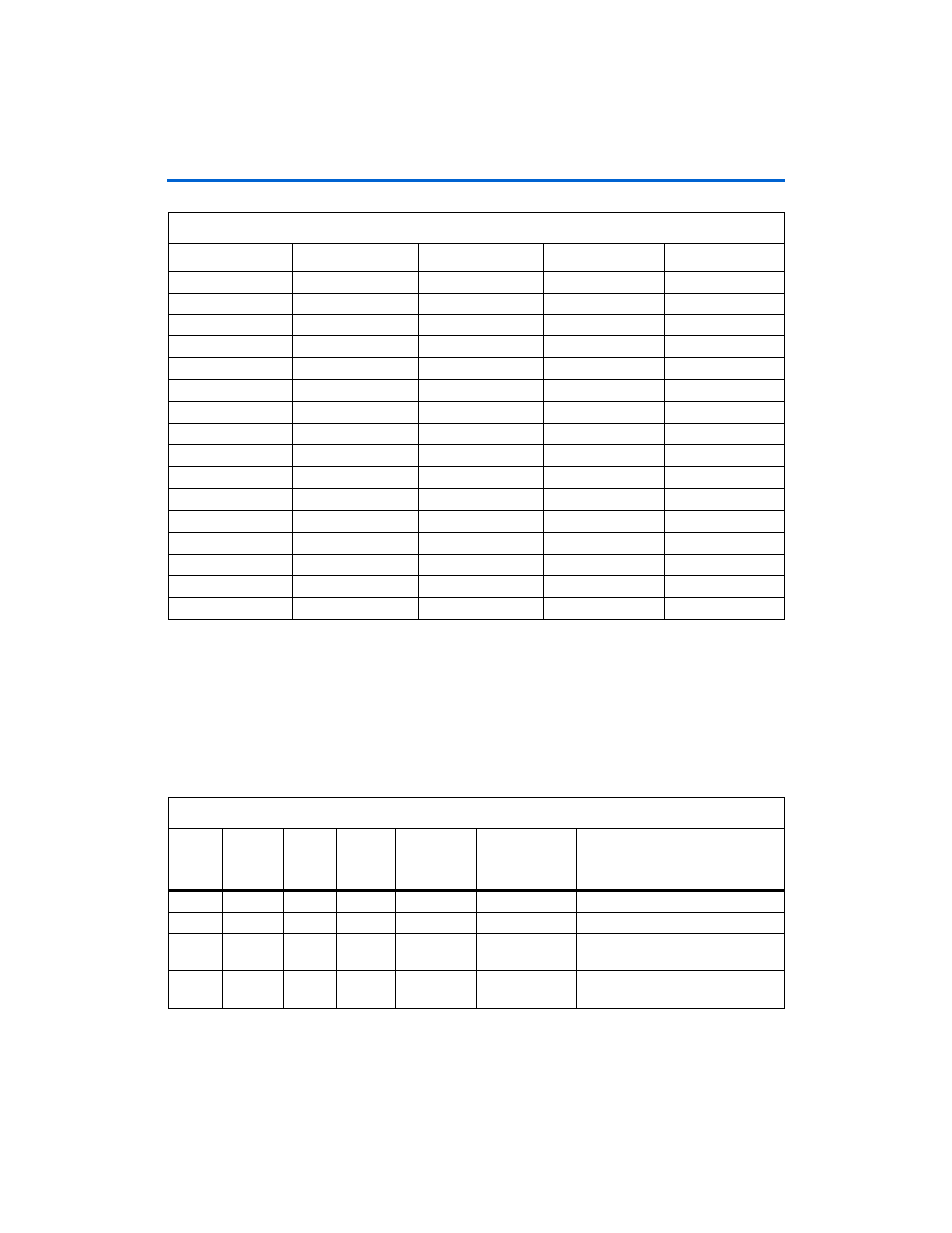
Table 2–17. Board Regulators
Output
Voltage
(V)
Variance
(+/- mV)
MAX
Current
(A)
Board
Access
Point
Regulator
Board
Reference
Linear
Technologies
Part #
Where Used
1.20
50
3.0
JP6
REG4
LT1959CS8
Cyclone III Core voltage
1.25
50
1.0
JP4
REG2
LTC3413
DDR termination voltage
2.50
50
6.0
JP3
REG1
LTM4603EV
DDR, SRAM, Flash, PLLs, other
bias voltages
1.80
80
1.5
JP7
REG5
LT1959CS8
Parallel flash interface, USB buffers
and other I/O