Chapter 3 – DFI CD9A3 series User Manual
Page 18
www.dfi .com
Chapter 3 Hardware Installation
18
Chapter 3
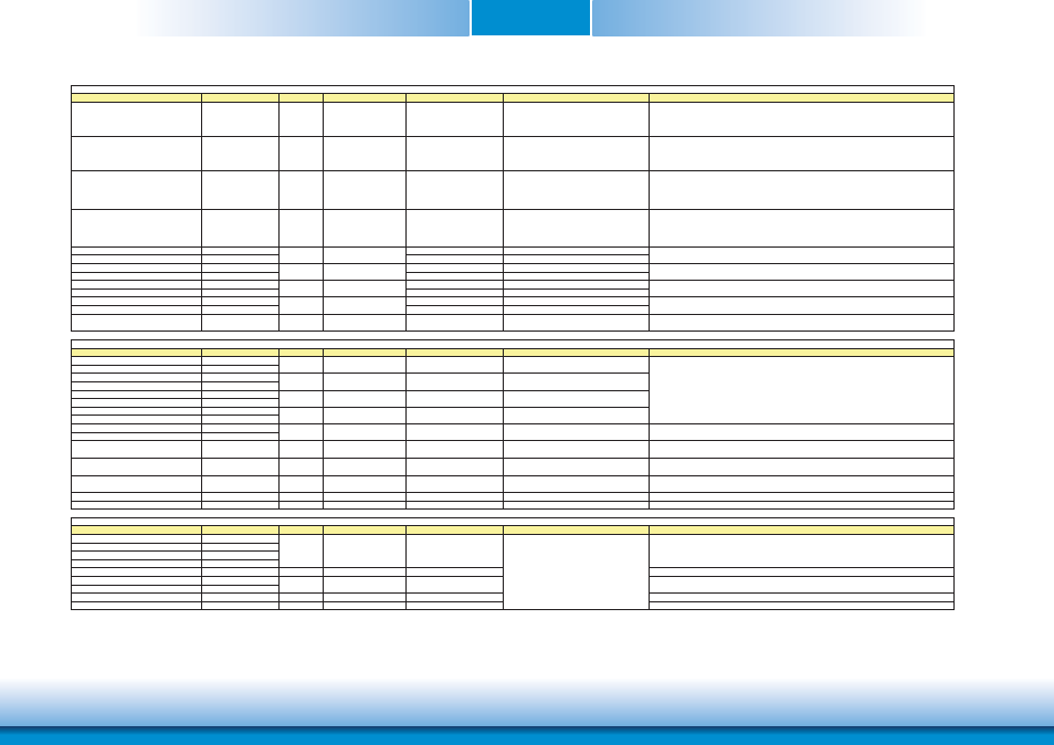
Signal
Pin#
Pin Type
Pwr Rail /Tolerance
CD9A3 Series
Carrier Board
Description
ȟ
ȟ
ȟ
ȟ
USB Signals Descriptions
USB_0_1_OC#
B44
I CMOS
3.3V Suspend/3.3V
PU 10k to 3.3VSB
Connect to Overcurrent of USB Power Switch
USB over-current sense, USB channels 0 and 1. A pull-up for this line
shall be present on the Module. An open drain driver from a USB
current monitor on the Carrier Board may drive this line low. Do not
pull this line high on the Carrier Board.
USB_2_3_OC#
A44
I CMOS
3.3V Suspend/3.3V
PU 10k to 3.3VSB
Connect to Overcurrent of USB Power Switch
USB over-current sense, USB channels 2 and 3. A pull-up for this line
shall be present on the Module. An open drain driver from a USB
current monitor on the Carrier Board may drive this line low. Do not
pull this line high on the Carrier Board.
USB_4_5_OC#
B38
I CMOS
3.3V Suspend/3.3V
PU 10k to 3.3VSB
Connect to Overcurrent of USB Power Switch
USB over-current sense, USB channels 4 and 5. A pull-up for this line
shall be present on the Module. An open drain driver from a USB
current monitor on the Carrier Board may drive this line low. Do not
pull this line high on the Carrier Board.
USB_6_7_OC#
A38
I CMOS
3.3V Suspend/3.3V
PU 10k to 3.3VSB
Connect to Overcurrent of USB Power Switch
USB over-current sense, USB channels 6 and 7. A pull-up for this line
shall be present on the Module. An open drain driver from a USB
current monitor on the Carrier Board may drive this line low. Do not
pull this line high on the Carrier Board.
USB_SSTX0+
D4
NA
NA
USB_SSTX0-
D3
NA
NA
USB_SSRX0+
C4
NA
NA
USB_SSRX0-
C3
NA
NA
USB_SSTX1+
D7
NA
NA
USB_SSTX1-
D6
NA
NA
USB_SSRX1+
C7
NA
NA
USB_SSRX1-
C6
NA
NA
USB_HOST_PRSNT
B96
I CMOS
3.3V Suspend/3.3V
NA
NA
Module USB client may detect the presence of a USB host. A high value(NA for CD9A3)
indicates that a host is present.
Signal
Pin#
Pin Type
Pwr Rail /Tolerance
CD9A3 Series
Carrier Board
Description
LVDS_A0+
A71
LVDS_A0-
A72
LVDS_A1+
A73
LVDS_A1-
A74
LVDS_A2+
A75
LVDS_A2-
A76
LVDS_A3+
A78
LVDS_A3-
A79
LVDS_A_CK+
A81
LVDS_A_CK-
A82
LVDS_VDD_EN
A77
O CMOS
3.3V / 3.3V
PD 100K to GND
Connect to enable control of LVDS panel power
circuit
LVDS panel power enable
LVDS_BKLT_EN
B79
O CMOS
3.3V / 3.3V
PD 100K to GND
Connect to enable control of LVDS panel backlight
power circuit.
LVDS panel backlight enable
LVDS_BKLT_CTRL
B83
O CMOS
3.3V / 3.3V
PD 100K to GND
Connect to brightness control of LVDS panel
backlight power circuit.
LVDS panel backlight brightness control
LVDS_I2C_CK
A83
I/O OD CMOS 3.3V / 3.3V
PU 2.2K to 3.3V
Connect to DDC clock of LVDS panel
I2C clock output for LVDS display use
LVDS_I2C_DAT
A84
I/O OD CMOS 3.3V / 3.3V
PU 2.2K to 3.3V
Connect to DDC data of LVDS panel
I2C data line for LVDS display use
Signal
Pin#
Pin Type
Pwr Rail /Tolerance
CD9A3 Series
Carrier Board
Description
LPC_AD0
B4
LPC_AD1
B5
LPC_AD2
B6
LPC_AD3
B7
LPC_FRAME#
B3
O CMOS
3.3V / 3.3V
LPC frame indicates the start of an LPC cycle
LPC_DRQ0#
B8
LPC_DRQ1#
B9
LPC_SERIRQ
A50
I/O CMOS
3.3V / 3.3V
PU 10K to 3.3V
LPC serial interrupt
LPC_CLK
B10
O CMOS
3.3V / 3.3V
LPC clock output - 33MHz nominal
ȟ
ȟ
ȟ
ȟ
I CMOS
LPC Signals Descriptions
I/O CMOS
3.3V / 3.3V
3.3V / 3.3V
LPC serial DMA request
LPC multiplexed address, command and data bus
Connect to LPC device
LVDS Channel A differential clock
O LVDS
LVDS
LVDS Signals Descriptions
O LVDS
LVDS
LVDS Channel A differential pairs
O LVDS
LVDS
O LVDS
LVDS
Connect to LVDS connector
Connect to LVDS connector
Connect to LVDS connector
Connect to LVDS connector
Connect to LVDS connector
O PCIE
AC coupled on Module
Additional transmit signal differential pairs for the SuperSpeed USB data path.(NA for CD9A3)
I PCIE
AC coupled off Modul
Additional receive signal differential pairs for the SuperSpeed USB data path.(NA for CD9A3)
O LVDS
LVDS
I PCIE
AC coupled off Modul
Additional receive signal differential pairs for the SuperSpeed USB data path.(NA for CD9A3)
O PCIE
AC coupled on Module
Additional transmit signal differential pairs for the SuperSpeed USB data path.(NA for CD9A3)