Chapter 3 – DFI CD9A3 series User Manual
Page 19
www.dfi .com
Chapter 3 Hardware Installation
19
Chapter 3
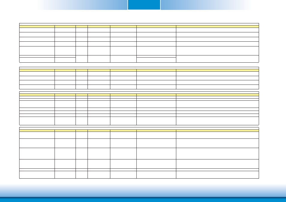
Signal
Pin#
Pin Type
Pwr Rail /Tolerance
CD9A3 Series
Carrier Board
Description
SPI_CS#
B97
O CMOS
3.3V Suspend/3.3V
Connect a series resistor 33ȟ to Carrier
Board SPI Device CS# pin
Chip select for Carrier Board SPI - may be sourced from chipset SPI0 or SPI1
SPI_MISO
A92
I CMOS
3.3V Suspend/3.3V
Connect a series resistor 33ȟ to Carrier
Board SPI Device SO pin
Data in to Module from Carrier SPI
SPI_MOSI
A95
O CMOS
3.3V Suspend/3.3V
Connect a series resistor 33ȟ to Carrier
Board SPI Device SI pin
Data out from Module to Carrier SPI
SPI_CLK
A94
O CMOS
3.3V Suspend/3.3V
Connect a series resistor 33ȟ to Carrier
Board SPI Device SCK pin
Clock from Module to Carrier SPI
SPI_POWER
A91
O
3.3V Suspend/3.3V
Power supply for Carrier Board SPI – sourced from Module – nominally
3.3V. The Module shall provide a minimum of 100mA on SPI_POWER.
Carriers shall use less than 100mA of SPI_POWER. SPI_POWER
shall only be used to power SPI devices on the Carrier
BIOS_DIS0#
A34
BIOS_DIS1#
B88
Signal
Pin#
Pin Type
Pwr Rail /Tolerance
CD9A3 Series
Carrier Board
Description
SER0_TX
A98
O CMOS
5V / 12V(design 3.3v~5V
tolerant)
PD 4.7K
General purpose serial port 0 transmitter
SER0_RX
A99
I CMOS
5V / 12V(design 3.3v~5V
tolerant)
PU 47K to 3.3V
General purpose serial port 0 receiver
SER1_TX
A101
O CMOS
5V / 12V(design 3.3v~5V
tolerant)
PD 4.7K
General purpose serial port 1 transmitter
SER1_RX
A102
I CMOS
5V / 12V(design 3.3v~5V
tolerant)
PU 47K to 3.3V
General purpose serial port 1 receiver
Signal
Pin#
Pin Type
Pwr Rail /Tolerance
CD9A3 Series
Carrier Board
Description
I2C_CK
B33
I/O OD CMOS 3.3V Suspend/3.3V
PU 2.2K to 3.3VSB
General purpose I2C port clock output
I2C_DAT
B34
I/O OD CMOS 3.3V Suspend/3.3V
PU 2.2K to 3.3VSB
General purpose I2C port data I/O line
SPKR
B32
O CMOS
3.3V / 3.3V
Output for audio enunciator - the "speaker" in PC-AT systems.
This port provides the PC beep signal and is mostly intended for
debugging purposes.
WDT
B27
O CMOS
3.3V / 3.3V
Output indicating that a watchdog time-out event has occurred.
FAN_PWNOUT
B101
O OD CMOS
3.3V / 12V
Fan speed control. Uses the Pulse Width Modulation (PWM) technique to control the fan's RPM.
FAN_TACHIN
B102
I OD CMOS
3.3V / 12V
Fan tachometer input for a fan with a two pulse output.
TPM_PP
A96
I CMOS
3.3V / 3.3V
Trusted Platform Module (TPM) Physical Presence pin. Active high.
TPM chip has an internal pull down. This signal is used to indicate
Physical Presence to the TPM.
(NC for CD9A3)
Signal
Pin#
Pin Type
Pwr Rail /Tolerance
CD9A3 Series
Carrier Board
Description
PWRBTN#
B12
I CMOS
3.3V Suspend/3.3V
PU 10K to 3.3VSB
A falling edge creates a power button event. Power button events can
be used to bring a system out of S5 soft off and other suspend states,
as well as powering the system down.
SYS_RESET#
B49
I CMOS
3.3V Suspend/3.3V
PU 10K to 3.3VSB
Reset button input. Active low request for Module to reset and reboot.
May be falling edge sensitive. For situations when SYS_RESET# is
not able to reestablish control of the system, PWR_OK or a power
cycle may be used.
CB_RESET#
B50
O CMOS
3.3V Suspend/3.3V
Reset output from Module to Carrier Board. Active low. Issued by
Module chipset and may result from a low SYS_RESET# input, a low
PWR_OK input, a VCC_12V power input that falls below the minimum
specification, a watchdog timeout, or may be initiated by the Module
software.
PWR_OK
B24
I CMOS
3.3V / 3.3V
PU 10K to 3.3V
Power OK from main power supply. A high value indicates that the
power is good. This signal can be used to hold off Module startup to
allow Carrier based FPGAs or other configurable devices time to be
programmed.
SUS_STAT#
B18
O CMOS
3.3V Suspend/3.3V
Indicates imminent suspend operation; used to notify LPC devices.
SUS_S3#
A15
O CMOS
3.3V Suspend/3.3V
Indicates system is in Suspend to RAM state. Active low output. An
inverted copy of SUS_S3# on the Carrier Board may be used to
enable the non-standby power on a typical ATX supply.
Serial Interface Signals Descriptions
Miscellaneous Signal Descriptions
NA
Selection straps to determine the BIOS boot device.
The Carrier should only float these or pull them low, please refer to
COM Express Module Base Specification Revision 2.1 for strapping options of BIOS disable signals.
SPI Signals Descriptions
I CMOS
Power and System Management Signals Descriptions