Chapter 3 – DFI CD9A3 series User Manual
Page 20
www.dfi .com
Chapter 3 Hardware Installation
20
Chapter 3
ȟ
ȟ
ȟ
ȟ
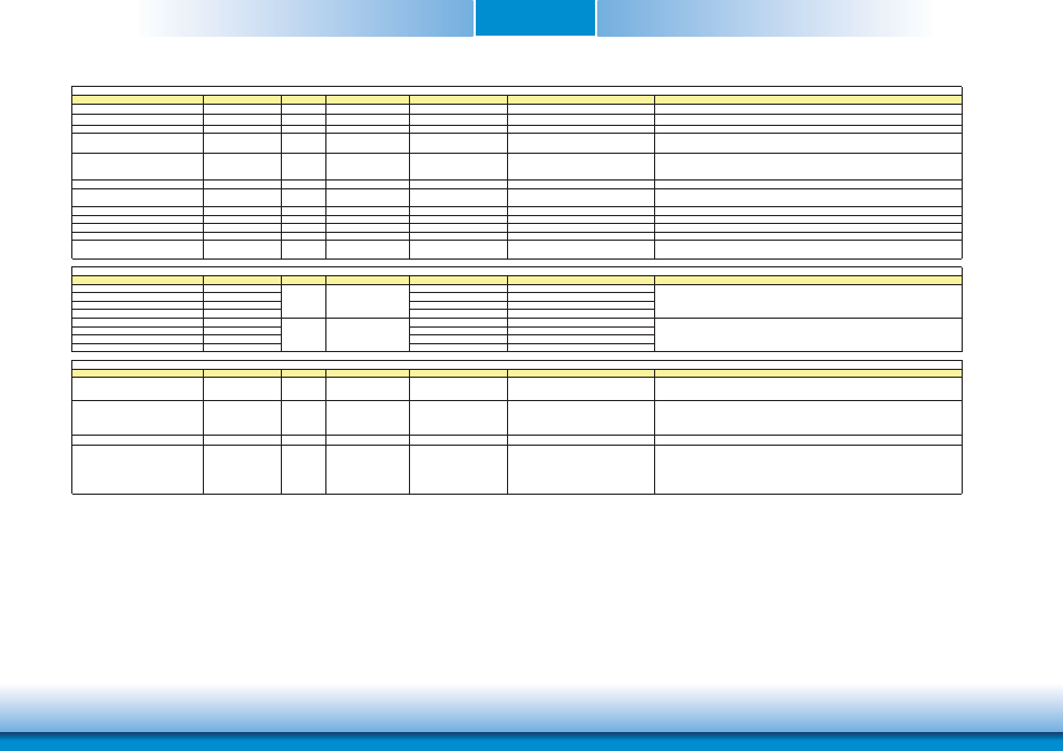
Signal
Pin#
Pin Type
Pwr Rail /Tolerance
CD9A3 Series
Carrier Board
Description
Power and System Management Signals Descriptions
ȟ
ȟ
ȟ
ȟ
SUS_S4#
A18
O CMOS
3.3V Suspend/3.3V
Indicates system is in Suspend to Disk state. Active low output.
SUS_S5#
A24
O CMOS
3.3V Suspend/3.3V
Indicates system is in Soft Off state.
WAKE0#
B66
I CMOS
3.3V Suspend/3.3V
PU 10K to 3.3VSB
PCI Express wake up signal.
WAKE1#
B67
I CMOS
3.3V Suspend/3.3V
PU 10K to 3.3VSB
General purpose wake up signal. May be used to implement wake-up
on PS2 keyboard or mouse activity.
BATLOW#
A27
I CMOS
3.3V Suspend/ 3.3V
PU 10K to 3.3VSB
Indicates that external battery is low.
This port provides a battery-low signal to the Module for orderly
transitioning to power saving or power cut-off ACPI modes.
LID#
A103
I OD CMOS
3.3V Suspend/12V
PU 10K to 3.3VSB
LID switch. Low active signal used by the ACPI operating system for a LID switch.
SLEEP#
B103
I OD CMOS
3.3V Suspend/12V
PU 10K to 3.3VSB
Sleep button. Low active signal used by the ACPI operating system to bring the
system to sleep state or to wake it up again.
THRM#
B35
I CMOS
3.3V / 3.3V
PU 10K to 3.3V
Input from off-Module temp sensor indicating an over-temp situation.
THRMTRIP#
A35
O CMOS
3.3V / 3.3V
PU 10K to 3.3V
Active low output indicating that the CPU has entered thermal shutdown.
SMB_CK
B13
I/O OD CMOS 3.3V Suspend/3.3V
PU 2.2K to 3.3VSB
System Management Bus bidirectional clock line.
SMB_DAT
B14
I/O OD CMOS 3.3V Suspend/3.3V
PU 2.2K to 3.3VSB
System Management Bus bidirectional data line.
SMB_ALERT#
B15
I CMOS
3.3V Suspend/3.3V
System Management Bus Alert – active low input can be used to
generate an SMI# (System Management Interrupt) or to wake the system.
Signal
Pin#
Pin Type
Pwr Rail /Tolerance
CD9A3 Series
Carrier Board
Description
GPO0
A93
GPO1
B54
GPO2
B57
GPO3
B63
GPI0
A54
PU 100K to 3.3V
GPI1
A63
PU 100K to 3.3V
GPI2
A67
PU 100K to 3.3V
GPI3
A85
PU 100K to 3.3V
Signal
Pin#
Pin Type
Pwr Rail /Tolerance
CD9A3 Series
Carrier Board
Description
VCC_12V
A104~A109
B104~B109
Power
4.75V – 20.0V
4.75V – 20.0V
Primary power input: +12V nominal. All available VCC_12V pins on the connector(s) shall be used.
The module supplies a wide range of power from 4.75V to 20.0V.
VCC_5V_SBY
B84~B87
Power
4.75V - 5.25V
4.75V - 5.25V
Standby power input: +5.0V nominal. If VCC5_SBY is used, all
available VCC_5V_SBY pins on the connector(s) shall be used. Only
used for standby and suspend functions. May be left unconnected if
these functions are not used in the system design.
VCC_RTC
A47
Power
2.0V - 3.3V
2.0V - 3.3V
Real-time clock circuit-power input. Nominally +3.0V.
GND
A1, A11, A21, A31, A41,
A51, A57, A60, A66, A70,
A80, A90, A100, A110, B1,
B11, B21 ,B31, B41, B51,
B60, B70, B80, B90, B100,
B110
Power
Ground - DC power and signal and AC signal return path.
All available GND connector pins shall be used and tied to Carrier
Board GND plane.
Power and GND Signal Descriptions
I CMOS
PU 100K to 3V3
General purpose input pins.
GPIO Signals Descriptions
O CMOS
3.3V / 3.3V
General purpose output pins.