Chapter 2 – DFI QB702-B User Manual
Page 15
www.dfi .com
Chapter 2 Hardware Installation
15
Chapter 2
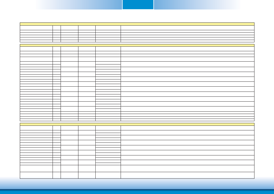
Signal
Pin#
Pin Type
Pwr Rail
/Tolerance
PU/PD (DFI-QB702)
Description
HDA_RST#
61
O CMOS
3.3V/3.3V
HD Audio/AC'97 Codec Reset.
HDA_SYNC
59
O CMOS
3.3V/3.3V
Serial Bus Synchronization
HDA_BCLK
63
O CMOS
3.3V/3.3V
HD Audio/AC'97 24 MHz Serial Bit Clock from Codec.
HDA_SDO
67
O CMOS
3.3V/3.3V
HD Audio/AC'97 Serial Data Output to Codec.
HDA_SDIN
65
I CMOS
3.3V/3.3V
HD Audio/AC'97 Serial Data input to Codec.
Signal
Pin#
Pin Type
Pwr Rail
/Tolerance
PU/PD (DFI-QB702)
Description
LVDS_PPEN
111
O CMOS
3.3V/3.3V
Controls panel power enable.
LVDS_BLEN
112
O CMOS
3.3V/3.3V
Controls panel Backlight enable.
LVDS_BLT_CTRL/GP_PWM_OUT0
123
O CMOS
3.3V/3.3V
Primary functionality is to control the panel backlight brightness via pulse width modulation (PWM).
When not in use for this primary purpose it can be used as General Purpose PWM Output.
LVDS_A0+
99
LVDS_A0-
101
LVDS_A1+
103
LVDS_A1-
105
LVDS_A2+
107
LVDS_A2-
109
LVDS_A3+
113
LVDS_A3-
115
LVDS_A_CLK+
119
LVDS_A_CLK-
121
LVDS_B0+
100
LVDS_B0-
102
LVDS_B1+
104
LVDS_B1-
106
LVDS_B2+
108
LVDS_B2-
110
LVDS_B3+
114
LVDS_B3-
112
LVDS_B_CLK+
120
LVDS_B_CLK-
122
LVDS_DID_CLK/GP_I2C_CLK
127
I/O OD CMOS
3.3V/3.3V
Primary functionality is DisplayID DDC clock line used for LVDS flat panel detection. If primary functionality is not used it can be as General Purpose I²C bus clock line.
LVDS_DID_DAT/GP_I2C_DAT
125
I/O OD CMOS
3.3V/3.3V
Primary functionality DisplayID DDC data line used for LVDS flat panel detection. If primary functionality is not used it can be as General Purpose I²C bus data line.
LVDS_BLC_CLK
128
I/O OD CMOS
3.3V/3.3V
Control clock signal for external SSC clock chip.
LVDS_BLC_DAT
126
I/O OD CMOS
3.3V/3.3V
Control data signal for external SSC clock chip.
Signal
Pin#
Pin Type
Pwr Rail
/Tolerance
PU/PD (DFI-QB702)
Description
SDVO_BCLK-
133
SDVO_BCLK+
131
SDVO_INT-
134
SDVO_INT+
132
SDVO_GREEN-
139
SDVO_GREEN+
137
SDVO_BLUE-
145
SDVO_BLUE+
143
SDVO_RED-
151
SDVO_RED+
149
SDVO_FLDSTALL-
140
SDVO_FLDSTALL+
138
SDVO_TVCLKIN-
146
SDVO_TVCLKIN+
144
SDVO_CTRL_CLK
152
I/O OD CMOS
3.3V/3.3V
I²C based control signal (clock) for SDVO device.
Note: If the control bus from the SDVO device has a different signaling voltage, then a level shifting device will be required on the carrier board to properly translate
the voltage level for this signal.
SDVO_CTRL_DAT
150
I/O OD CMOS
3.3V/3.3V
I²C based control signal (data) for SDVO device.
Note: If the control bus from the SDVO device has a different signaling voltage, then a level shifting device will be required on the carrier board to properly translate
the voltage level for this signal.
SDVO differential pair red data lines.
SDVO differential pair field stall lines.
SDVO differential pair TV-Out synchronization clock lines.
O PCIE
I PCIE
O PCIE
O PCIE
O PCIE
I PCIE
I PCIE
SDVO Interface Signals
SDVO differential pair clock lines.
SDVO differential pair interrupt input lines.
SDVO differential pair green data lines.
SDVO differential pair blue data lines.
SDVO
SDVO
SDVO
SDVO
SDVO
SDVO
SDVO
O LVDS
O LVDS
High Definition Audio Signals/AC'97
LVDS Flat Panel Signals
LVDS primary channel differential pair 0.
O LVDS
O LVDS
LVDS primary channel differential pair 1.
LVDS primary channel differential pair 2.
LVDS
LVDS
LVDS
LVDS secondary channel differential pair 3.
O LVDS
LVDS secondary channel differential pair clock lines.
LVDS primary channel differential pair 3.
O LVDS
LVDS primary channel differential pair clock lines.
O LVDS
LVDS secondary channel differential pair 0.
O LVDS
LVDS secondary channel differential pair 1.
O LVDS
LVDS secondary channel differential pair 2.
O LVDS
LVDS
LVDS
LVDS
LVDS
LVDS
LVDS
LVDS