Chapter 2 – DFI QB702-B User Manual
Page 17
www.dfi .com
Chapter 2 Hardware Installation
17
Chapter 2
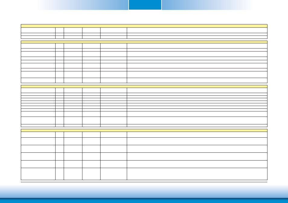
Signal
Pin#
Pin Type
Pwr Rail
/Tolerance
PU/PD (DFI-QB702)
Description
PWGIN
26
I CMOS
5V/5V
High active input for the Qseven® module indicates that all power rails located on the carrier board are ready for use.
PWRBTN#
20
I CMOS
3.3V Standby
Power Button: Low active power button input. This signal is triggered on the falling edge.
Signal
Pin#
Pin Type
Pwr Rail
/Tolerance
PU/PD (DFI-QB702)
Description
RSTBTN#
28
I CMOS
3.3V/3.3V
Reset button input. This input may be driven active low by an external circuitry to reset the Qseven module.
BATLOW#
27
I CMOS
3.3V Suspend/3.3V
PU 10K to 3.3V Suspend
Battery low input. This signal may be driven active low by external circuitry to signal that the system battery is low or may be used to signal some other external
battery management event.
WAKE#
17
I CMOS
3.3V Suspend/3.3V
PU 10K to 3.3V Suspend
External system wake event. This may be driven active low by external circuitry to signal an external wake-up event.
SUS_STAT#
19
O CMOS
3.3V Suspend/3.3V
PU 10K to 3.3V Suspend
Suspend Status: indicates that the system will be entering a low power state soon.
SUS_S3#
18
O CMOS
3.3V Suspend/3.3V
S3 State: This signal shuts off power to all runtime system components that are not maintained during S3 (Suspend to Ram), S4 or S5 states.
The signal SUS_S3# is necessary in order to support the optional S3 cold power state.
SUS_S5#
16
O CMOS
3.3V Suspend/3.3V
S5 State: This signal indicates S4 or S5 (Soft Off) state.
SLP_BTN#
21
I CMOS
3.3V Suspend/3.3V
PU 10K to 3.3V Suspend
Sleep button. Low active signal used by the ACPI operating system to transition the system into sleep state or to wake it up again. This signal is triggered on falling
edge.
LID_BTN#
22
I CMOS
3.3V Suspend/3.3V
PU 10K to 3.3V Suspend
LID button. Low active signal used by the ACPI operating system to detect a LID switch and to bring system into sleep state or to wake it up again.
Open/Close state may be software configurable.
Signal
Pin#
Pin Type
Pwr Rail
/Tolerance
PU/PD (DFI-QB702)
Description
WDTRIG#
70
I CMOS
3.3V/3.3V
Watchdog trigger signal. This signal restarts the watchdog timer of the Qseven module on the falling edge of a low active pulse.
WDOUT
72
O CMOS
3.3V/3.3V
Watchdog event indicator. High active output used for signaling a missing watchdog trigger. Will be deasserted by software, system reset or a system power down.
I2C_CLK
66
I/O OD CMOS
3.3V/3.3V
PU 10K to 3.3V
Clock line of I²C bus.
I2C_DAT
68
I/O OD CMOS
3.3V/3.3V
PU 10K to 3.3V
Data line of I²C bus.
SMB_CLK
60
I/O OD CMOS
3.3V Suspend/3.3V
PU 2K to 3.3V Suspend
Clock line of System Management Bus.
SMB_DAT
62
I/O OD CMOS
3.3V Suspend/3.3V
PU 2K to 3.3V Suspend
Data line of System Management Bus.
SMB_ALERT#
64
O CMOS
3.3V/3.3V
PU 2K to 3.3V Suspend
System Management Bus Alert input. This signal may be driven low by SMB devices to signal an event on the SM Bus.
SPKR/GP_PWM_OUT2
194
O CMOS
3.3V/3.3V
Primary functionality is output for audio enunciator, the“speaker” in PC AT systems. When not in use for this primary purpose it can be used as General Purpose PWM
Output.
BIOS_DISABLE#/BOOT_ALT#
41
I CMOS
3.3V/3.3V
Module BIOS disable input signal. Pull low to disable module's on-board BIOS.
Allows off-module BIOS implementations. This signal can also be used to disable standard boot firmware flash device and enable an alternative boot firmware source, for
example a boot loader.
RSVD
56,124,
NC
Do not connect
Signal
Pin#
Pin Type
Pwr Rail
/Tolerance
PU/PD (DFI-QB702)
Description
MFG_NC0
207
N.A
N.A
This pin is reserved for manufacturing and debugging purposes.
May be used as JTAG_TCK signal for boundary scan purposes during production or as a vendor specific control signal. When used as a vendor specific control signal the
multiplexer must be controlled by the MFG_NC4 signal.
MFG_NC1
209
N.A
N.A
This pin is reserved for manufacturing and debugging purposes.
May be used as JTAG_TDO signal for boundary scan purposes during production. May also be used, via a multiplexer, as a UART_TX signal to connect a simple UART for
firmware and boot loader implementations. In this case the multiplexer must be controlled by the MFG_NC4 signal.
MFG_NC2
208
N.A
N.A
This pin is reserved for manufacturing and debugging purposes.
May be used as JTAG_TDI signal for boundary scan purposes during production. May also be used, via a multiplexer, as a UART_RX signal to connect a simple UART for
firmware and boot loader implementations. In this case the multiplexer must be controlled by the MFG_NC4 signal.
MFG_NC3
210
N.A
N.A
This pin is reserved for manufacturing and debugging purposes.
May be used as JTAG_TMS signal for boundary scan purposes during production. May also be used, via a multiplexer, as vendor specific BOOT signal for firmware and
boot loader implementations. In this case the multiplexer must be controlled by the MFG_NC4 signal.
MFG_NC4
204
N.A
N.A
This pin is reserved for manufacturing and debugging purposes.
May be used as JTAG_TRST# signal for boundary scan purposes during production. May also be used as control signal for a multiplexer circuit on the module enabling
secondary function for MFG_NC0..3 ( JTAG / UART ).
When MFG_NC4 is high active it is being used for JTAG purposes.
When MFG_NC4 is low active it is being used for UART purposes.
Power Management Signals
Miscellaneous Signals
Manufacturing Signals
Power Control Signals