Xilinx fpga – Sundance SMT364 User Manual
Page 28
Version 1.0
Page 28 of 37
SMT364 User Manual
(“110”) or 12 (“111”). See
ICS8430-01
datasheet for more information performance,
jitter, etc.
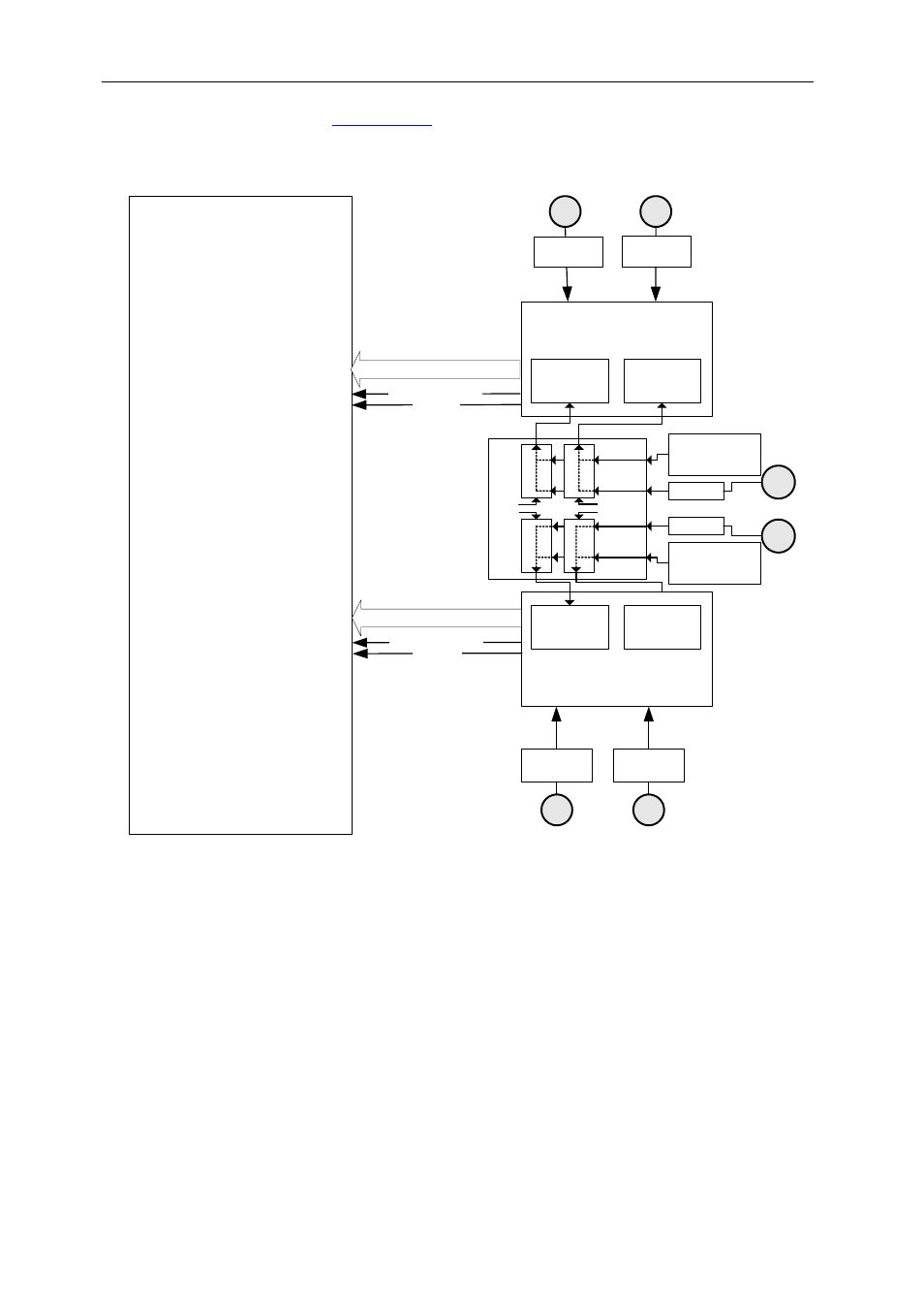
The following diagram shows how clock signals can be routed on the PCB.
A and B
Xilinx
FPGA
Virtex-II, FG456
XC2V1000-6
324 I/O Pins
1.5V Core
3.3V I/O
#1
AC or DC
coupling
2xAD6645 ADCs
14-bit @ 105MSPS
52-pin LQFP
30 I/O pins; 28-bit data; ctl
#4
#3
RF
transformer
#2
Clock feedbacks
Clk
1
opamp
opamp
Clock synthe-
sizer
ADCA&B
Clk
2
AC or DC
coupling
ADC A
ADC B
Clock synthe-
sizer
ADCC&D
Bit25
0
1
Bit24
0
1
0
1
0
1
Bit27
Bit26
RF
transformer
2xAD6645 ADCs
14-bit @ 105MSPS
52-pin LQFP
ADC C
ADC D
C and D
30 I/O pins; 28-bit data; ctl
Clock feedbacks
Figure 9 - Clock Routing.
The skew between ADC clock signals is negligible, which means that samples
coming from both converters can be considered as synchronised when Bit26 and
Bit27 are the same.