Sundance SMT364 User Manual
Page 9
Version 1.0
Page 9 of 37
SMT364 User Manual
Virtex FPGA.
What the FPGA does.
The SMT364 is populated with a Xilinx Virtex FPGA (
XC2V1000-4FG456
). This
device controls major functions on the module, like CommPorts and SHB
communications, data flows from the converters and clock management.
This FPGA needs being configured after power-up and after a module reset. This
operation is possible thanks to the on-board Xilinx PROM. This operation can be
done automatically when jumper J1 (Figure 8 - Connector Location.) is fitted. If it is
not fitted, no configuration is loaded into the FPGA and allows therefore the user to
program the FPGA via JTAG with no possible conflict.
Four control registers are implemented into this FPGA to set up converters, their data
format, clock synthesizers, CommPort and SHB. Some more details are given in the
next parts of this document.
The FPGA is serially programmed using the dedicated pins. The PROM is originally
programmed with a default bit stream, which implements all features mentioned in
this document.
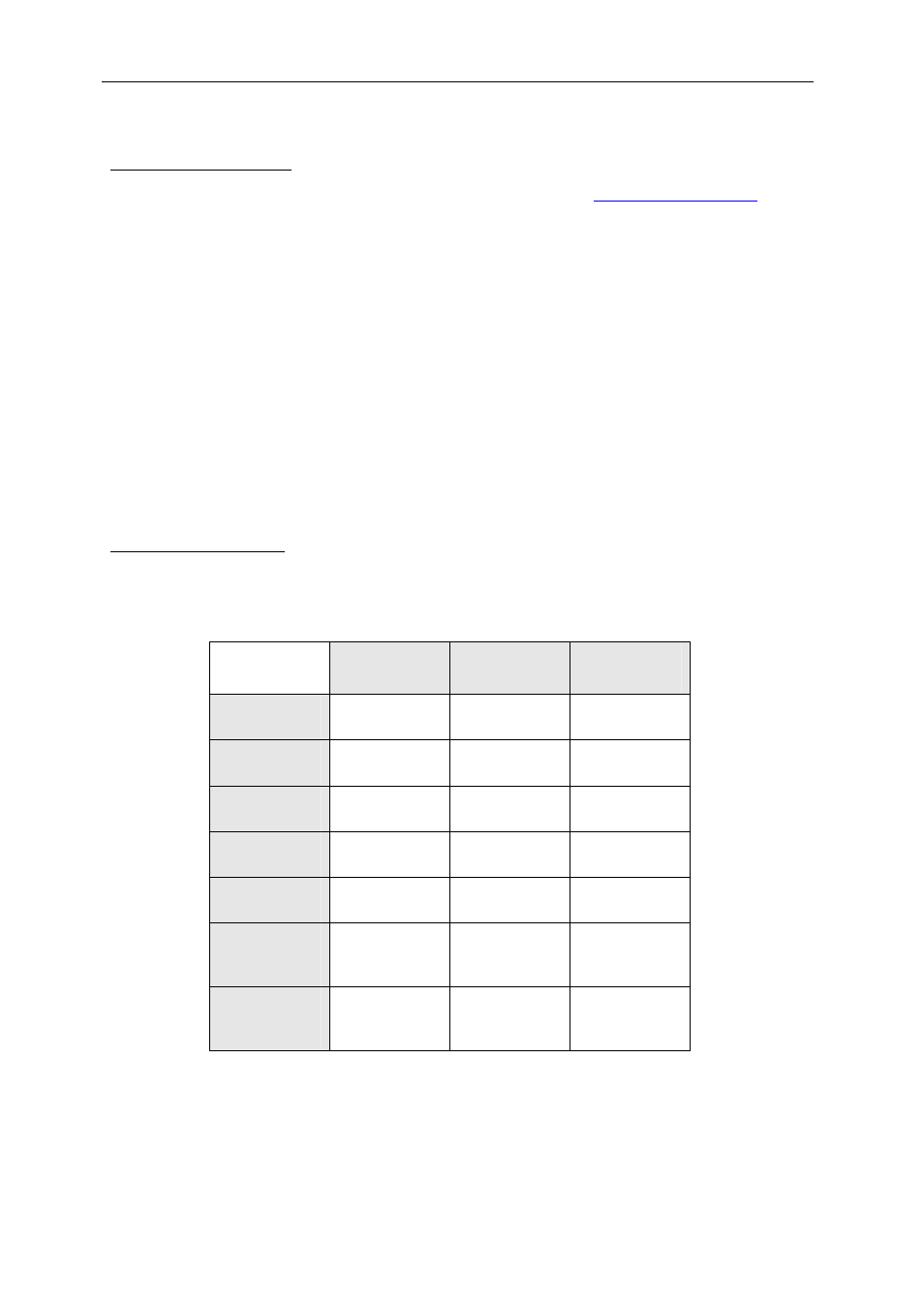
Ressource occupied.
The default firmware, as it comes with the board, uses FPGA resources, such as
Ram Blocks, Flip-flop, Slices, I/O pads. The following table gathers all of them:
Number
used
Out of
Percentage
of utilisation
Number of
External IOBs
170
324
52%
Number of
RAMB16s
0
40
0%
Number of
SLICEs
753
5120
14%
Number of
GCLKs
5
16
31%
Number of
DCMs
0
8
0%
Number of
External
DIFFMs
0
162
0%
Number of
External
DIFFSs
0
162
0%
Figure 2 - FPGA utilisation.