Connector pinouts, Fpga jtag (jp1), Fpga prog pin control (jp2) – Sundance SMT395 User Manual
Page 19
Advertising
Version 1.1.7
Page 19 of 26
SMT395 User Manual
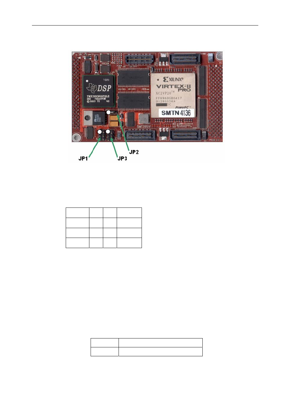
Connector Pinouts
FPGA JTAG (JP1)
The following shows the pin-outs for JP1 (FPGA) JTAG connector:
Signal Pin Pin Signal
V33 1 4 TDI
TMS 2 5 TDO
TCK 3 6 GND
Note: The Pin 1 is marked by a white mark on the silkscreen (see white spot on the
previous picture).
FPGA PROG Pin Control (JP2)
The FPGA PROG pin is used to clear the FPGA configuration.
It is to be used as a safety in case the FPGA has been programmed with a bad
bitstream that corrupts the dsp external bus and prevents which any further
programming. Changing the jumper allows the user to clear the FPGA configuration
and reprogram the FPGA.
1-2
PROG under control of DSP
2-3 or out
PROG asserted
Advertising