Block diagram, Architecture description, Fpga controller – Sundance SMT395 User Manual
Page 7
Version 1.1.7
Page 7 of 26
SMT395 User Manual
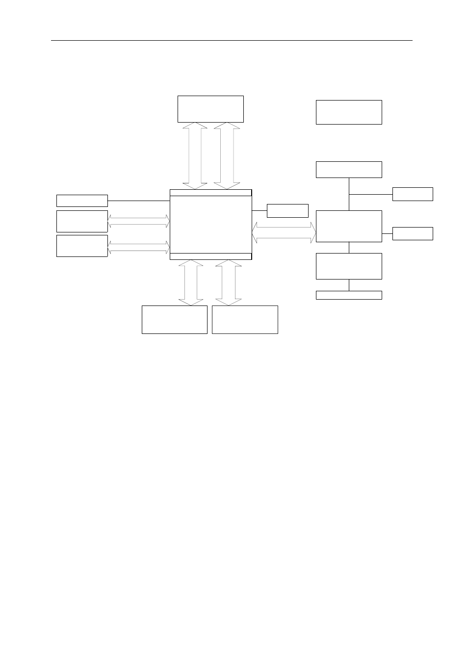
Block Diagram
2
x
C
o
mm
-P
ort
s
/S
D
L
Clocks,
T
imer, In
ter
ru
p
ts, PX
I.
4
x
C
o
m
m
-Po
rt/SD
L
G
lob
al B
u
s
104 I/O pins
133MHz EMIFA
FPGA Controller
Virtex-II Pro, FF896
XC2VP20,30
1
.5V Core
3.3V I/O
DSP
1GHz 'C6416
525 pins - 1.4V
JTAG Header
J1 Top Primary TIM
Connector
Comm-Port 0 & 3
J3 Global Expansion
Connector
J2 Bottom Primary TIM
Connector
Comm-Port 1, 2, 4 & 5
McBSP/Utopia/GPIO
(all non-TIM I/O pins)
4 LEDs &
4 I/O pins
8Mbyte Flash (EMIFB CE1)
4 LEDs
Oscillators
DC-DC Converters
1.5V & 1.4V
256Mbytes SDRAM
(4 x 32M x16 133MHz)
EMIFA
2 x Sundance High-
speed Bus (SHB)
60-way Samtec QSH
120 I/O Pins; 32-bit Data
5V<>3V3 level translator
5V<>3V3 level translator
2 x Sundance RSL
connectors (Xilinx
Rocket-IO)
28-way Samtec QxE
8 differential serial links
Architecture Description
The SMT395 TIM consists of a Texas Instruments TMS320C6416T running at up to
1GHz. Modules are populated with 256MBytes of SDRAM.
A Field Programmable Gate Array (FPGA) is used to manage global bus accesses
and implement six communication ports and two Sundance High Speed Buses. This
is a Xilinx VirtexII-Pro device.