Timer, Timer control register – Sundance SMT335E User Manual
Page 37
Advertising
Version 1.5
Page 37 of 53
SMT335E SMT375E User Manual
Timer
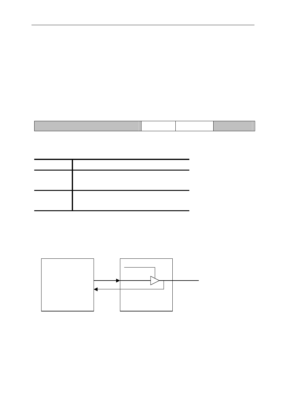
The TIM TCLK0 and TCLK1 signals can be routed to the DSP’s TOUT/TINP pins.
The signal direction must be specified, together with the routing information in the
timer control register.
Timer Control Register
TCLK 0x03C00000
31–6 5
4
3–0
TCLK1 EN
TCLK9 EN
RW,0 RW,0
Field Description
0 TIM TCLK0 is an input
TCLK0EN
1 Enable TIM TCLK0 as an output
0 TIM TCLK1 is an input
TCLK1EN
1 Enable TIM TCLK1 as an output
If the TIM TCLKx pin is selected as an output, the C6000 TOUTx signal will be used
to drive it. The TIM TCLKx pin will always drive the C6000 TINPx input.
FPGA
TOUT0
TCLK0
TCLK0EN
TINP0
C6x
Advertising
This manual is related to the following products: