Interference considerations, Pad layout, Board layout guidelines – Linx Technologies TRM-xxx-NT User Manual
Page 16
– –
– –
26
27
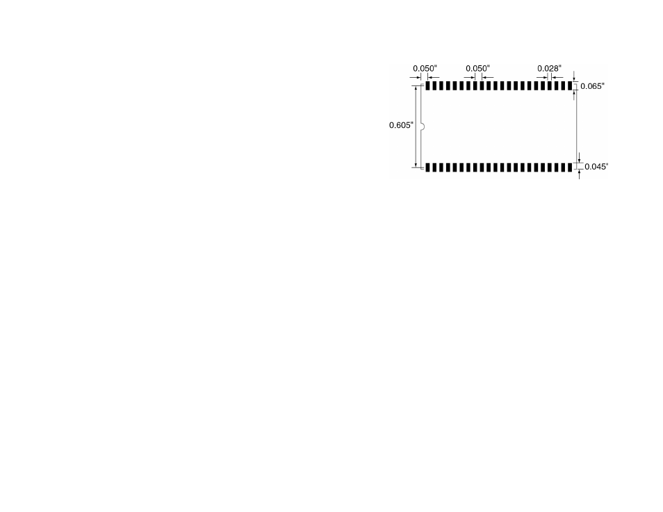
Pad Layout
The pad layout diagram in Figure 32 is designed to facilitate both hand and
automated assembly.
Board Layout Guidelines
The module’s design makes integration straightforward; however, it is
still critical to exercise care in PCB layout. Failure to observe good layout
techniques can result in a significant degradation of the module’s
performance. A primary layout goal is to maintain a characteristic 50-ohm
impedance throughout the path from the antenna to the module.
Grounding, filtering, decoupling, routing and PCB stack-up are also
important considerations for any RF design. The following section provides
some basic design guidelines which may be helpful.
During prototyping, the module should be soldered to a properly laid-out
circuit board. The use of prototyping or “perf” boards will result in poor
performance and is strongly discouraged. Likewise, the use of sockets
can have a negative impact on the performance of the module and
are discouraged.
The module should, as much as reasonably possible, be isolated from
other components on your PCB, especially high-frequency circuitry such
as crystal oscillators, switching power supplies, and high-speed bus lines.
When possible, separate RF and digital circuits into different PCB regions.
Make sure internal wiring is routed away from the module and antenna and
is secured to prevent displacement.
Figure 32: Recommended PCB Layout
Interference Considerations
The RF spectrum is crowded and the potential for conflict with other
unwanted sources of RF is very real. While all RF products are at risk
from interference, its effects can be minimized by better understanding its
characteristics.
Interference may come from internal or external sources. The first step
is to eliminate interference from noise sources on the board. This means
paying careful attention to layout, grounding, filtering and bypassing in
order to eliminate all radiated and conducted interference paths. For
many products, this is straightforward; however, products containing
components such as switching power supplies, motors, crystals and other
potential sources of noise must be approached with care. Comparing your
own design with a Linx evaluation board can help to determine if and at
what level design-specific interference is present.
External interference can manifest itself in a variety of ways. Low-level
interference will produce noise and hashing on the output and reduce the
link’s overall range.
High-level interference is caused by nearby products sharing the same
frequency or from near-band high-power devices. It can even come from
your own products if more than one transmitter is active in the same area.
It is important to remember that only one transmitter at a time can occupy
a frequency, regardless of the coding of the transmitted signal. This type of
interference is less common than those mentioned previously, but in severe
cases it can prevent all useful function of the affected device.
Although technically not interference, multipath is also a factor to be
understood. Multipath is a term used to refer to the signal cancellation
effects that occur when RF waves arrive at the receiver in different phase
relationships. This effect is a particularly significant factor in interior
environments where objects provide many different signal reflection paths.
Multipath cancellation results in lowered signal levels at the receiver and
shorter useful distances for the link.