Microstrip details – Linx Technologies TRM-xxx-NT User Manual
Page 17
– –
– –
28
29
Microstrip Details
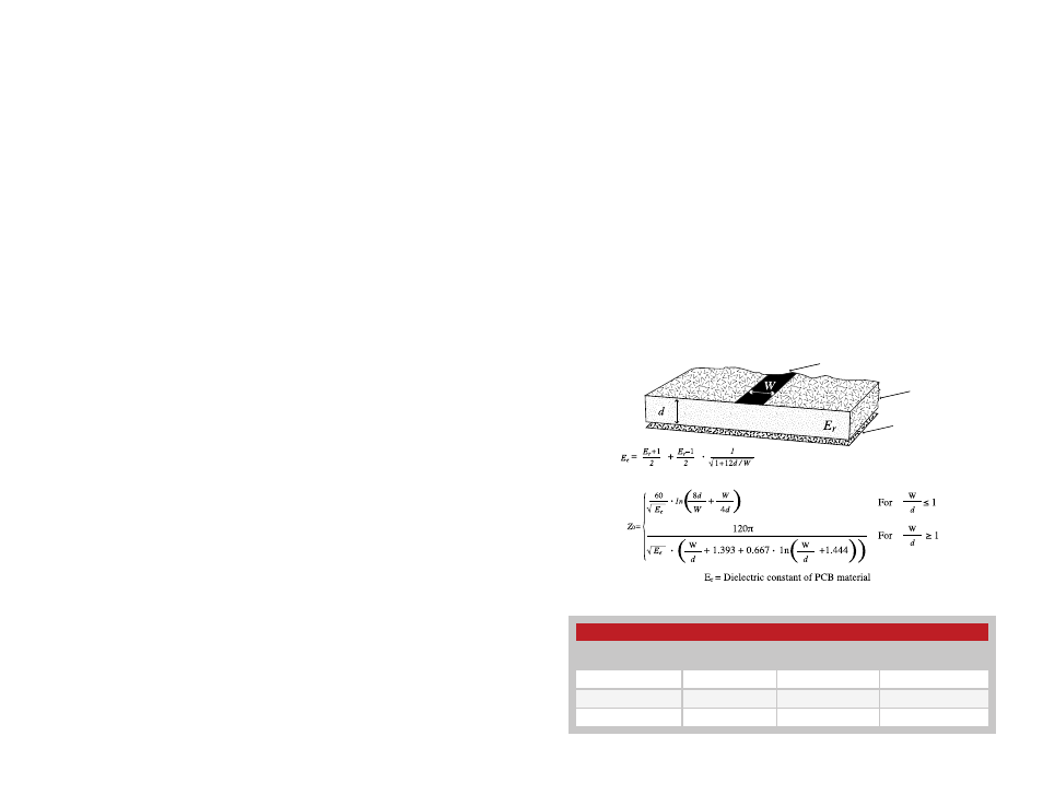
A transmission line is a medium whereby RF energy is transferred from
one place to another with minimal loss. This is a critical factor, especially
in high-frequency products like Linx RF modules, because the trace
leading to the module’s antenna can effectively contribute to the length
of the antenna, changing its resonant bandwidth. In order to minimize
loss and detuning, some form of transmission line between the antenna
and the module should be used unless the antenna can be placed very
close (<1/8in) to the module. One common form of transmission line is a
coax cable and another is the microstrip. This term refers to a PCB trace
running over a ground plane that is designed to serve as a transmission line
between the module and the antenna. The width is based on the desired
characteristic impedance of the line, the thickness of the PCB and the
dielectric constant of the board material. For standard 0.062in thick FR-4
board material, the trace width would be 111 mils. The correct trace width
can be calculated for other widths and materials using the information in
Figure 33 and examples are provided in Figure 34. Software for calculating
microstrip lines is also available on the Linx website.
Trace
Board
Ground plane
Figure 33: Microstrip Formulas
Example Microstrip Calculations
Dielectric Constant
Width / Height
Ratio (W / d)
Effective Dielectric
Constant
Characteristic
Impedance (Ω)
4.80
1.8
3.59
50.0
4.00
2.0
3.07
51.0
2.55
3.0
2.12
48.8
Figure 34: Example Microstrip Calculations
Do not route PCB traces directly under the module. There should not be
any copper or traces under the module on the same layer as the module,
just bare PCB. The underside of the module has traces and vias that could
short or couple to traces on the product’s circuit board.
The Pad Layout section shows a typical PCB footprint for the module.
A ground plane (as large and uninterrupted as possible) should be placed
on a lower layer of your PC board opposite the module. This plane is
essential for creating a low impedance return for ground and consistent
stripline performance.
Use care in routing the RF trace between the module and the antenna or
connector. Keep the trace as short as possible. Do not pass it under the
module or any other component. Do not route the antenna trace on
multiple PCB layers as vias will add inductance. Vias are acceptable for
tying together ground layers and component grounds and should be used
in multiples.
Each of the module’s ground pins should have short traces tying
immediately to the ground plane through a via.
Bypass caps should be low ESR ceramic types and located directly
adjacent to the pin they are serving.
A 50-ohm coax should be used for connection to an external antenna.
A 50-ohm transmission line, such as a microstrip, stripline or coplanar
waveguide should be used for routing RF on the PCB. The Microstrip
Details section provides additional information.
In some instances, a designer may wish to encapsulate or “pot” the
product. There are a wide variety of potting compounds with varying
dielectric properties. Since such compounds can considerably impact RF
performance and the ability to rework or service the product, it is the
responsibility of the designer to evaluate and qualify the impact and
suitability of such materials.