Scsi input, Data latch (sidl), Scsi input data latch (sidl) – Avago Technologies LSI8751D User Manual
Page 193: Scsi, Input data latch (sidl), Scsi input data, Latch (sidl), Scsi input data latch, Sidl)
5-77
, and SODR full bits in the
and
are cleared.
STW
SCSI FIFO Test Write
0
Setting this bit places the SCSI core into a test mode in
which the FIFO is easily read or written. While this bit is
set, writes to the least significant byte of the
register cause the entire word
contained in this register to be loaded into the FIFO.
Writing the least significant byte of the
register will cause the FIFO to load. These
functions are summarized in the table below.
Register: 0x50–0x51 (0xD0–0xD1)
SCSI Input Data Latch (SIDL)
Read Only
SIDL
SCSI Input Data Latch
[15:0]
This register is used primarily for diagnostic testing,
programmed I/O operation, or error recovery. Data
received from the SCSI bus can be read from this
register. Data can be written to the
register and then read back into the
LSI53C875 by reading this register to allow loopback
testing. When receiving SCSI data, the data flows into
this register and out to the host FIFO. This register differs
from the
register;
contains latched data and the
always contains exactly
what is currently on the SCSI data bus. The power-up
value of this register is indeterminate.
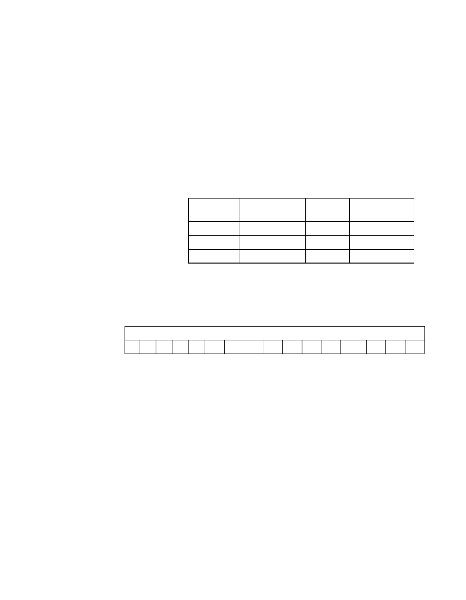
Register
Name
Register
Operation
FIFO Bits
FIFO
Function
SODL
Write
[15:0]
Load
SODL0
Write
[7:0]
Load
SODL1
Write
[15:8]
None
15
0
SIDL
x
x
x
x
x
x
x
x
x
x
x
x
x
x
x
x