Recommended operating conditions, Thermal impedance – Diodes AP3988/89/90 User Manual
Page 4
AP3988/89/90
Document number: DS36722 Rev. 3 - 2
4 of 13
www.diodes.com
March 2014
© Diodes Incorporated
AP3988/89/90
A Product Line of
Diodes Incorporated
N
E
W
P
R
O
D
U
C
T
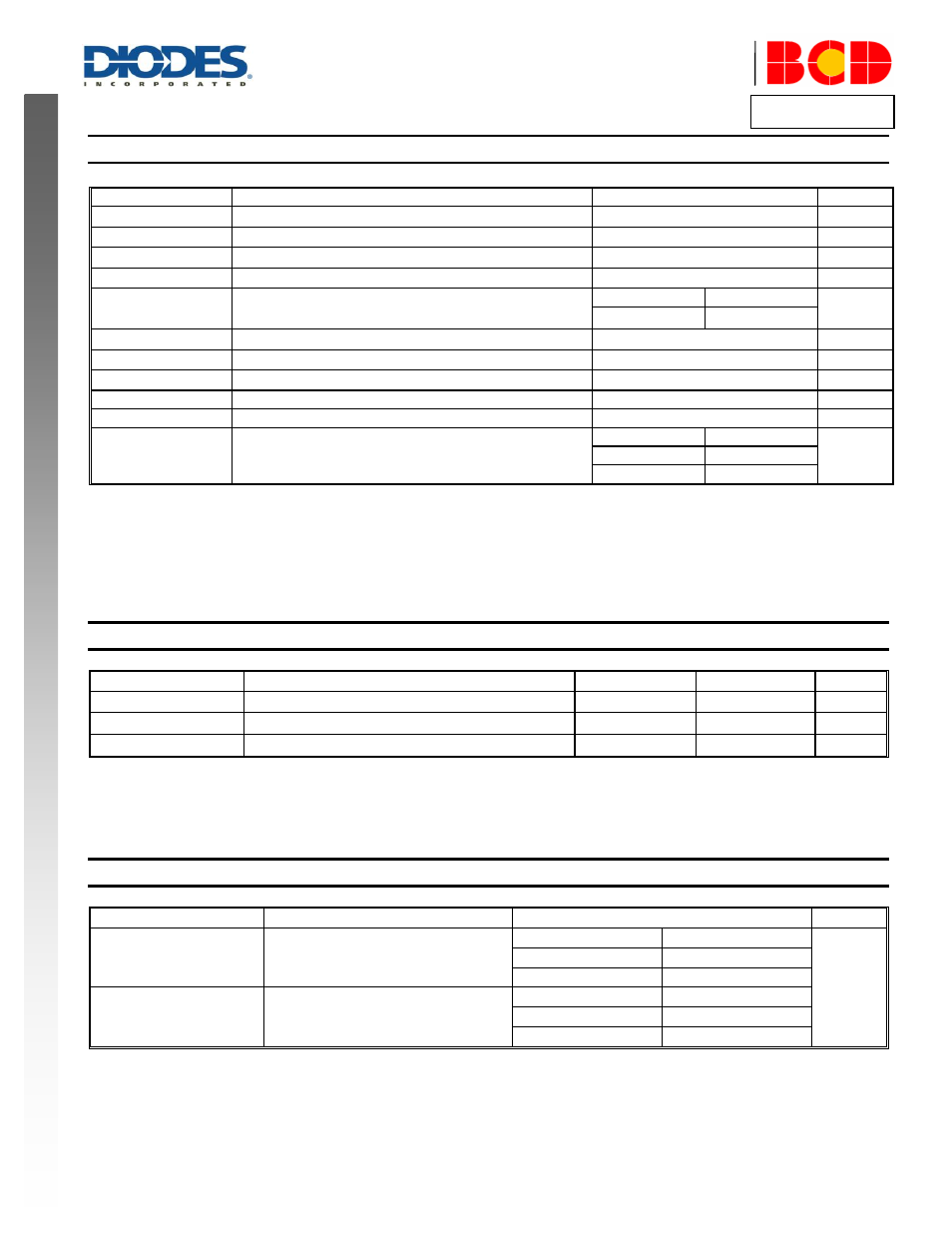
Absolute Maximum Ratings
(Note 5)
Symbol
Parameter
Rating
Unit
V
CC
Supply Voltage
-0.3 to 30
V
V
CS
, V
CPC
Voltage on CS, CPC Pin
-0.3 to 7
V
V
FB
FB Input Voltage
-0.3 to 8
V
V
CBO
Collector-emitter Voltage
700
V
I
CDC
Collector DC Current
AP3988/89
1.5
A
AP3990
4
T
J
Operating Junction Temperature
+150
°C
T
STG
Storage Temperature
-65 to +150
°C
T
LEAD
Lead Temperature (Soldering, 10 sec)
+300
°C
–
ESD (Machine Model)
200
V
–
ESD (Human Body Model)
2000
V
P
D
Total Power Dissipation
AP3988
0.7
W
AP3989
0.9
AP3990
1.1
Note 5
: Stresses greater than those listed under “Absolute Maximum Ratings” may cause permanent damage to the device. These are stress ratings only, and
functional operation of the device at these or any other conditions beyond those indicated under “Recommended Operating Conditions” is not implied.
Exposure to “Absolute Maximum Ratings” for extended periods may affect device reliability.
Recommended Operating Conditions
Symbol
Parameter
Min
Max
Unit
V
CC
Supply Voltage
–
25
V
T
OP
Operating Temperature Range
-40
+85
°C
f
S(MAX)
Maximum Operating Frequency
–
60
kHz
Thermal Impedance
(Note 6)
Symbol
Parameter
Value
Unit
θ
JA
Junction to Ambient
AP3988
100
°C/W
AP3989
80
AP3990
65
θ
JC
Junction to Case
AP3988
50
AP3989
40
AP3990
35
Note 6: When mounted a standard single-sided FR4 board with 300mm
2
Cu (at least 35µm thick) connected to all collectors and CS pins.