Diodes AP3988/89/90 User Manual
Page 5
AP3988/89/90
Document number: DS36722 Rev. 3 - 2
5 of 13
www.diodes.com
March 2014
© Diodes Incorporated
AP3988/89/90
A Product Line of
Diodes Incorporated
N
E
W
P
R
O
D
U
C
T
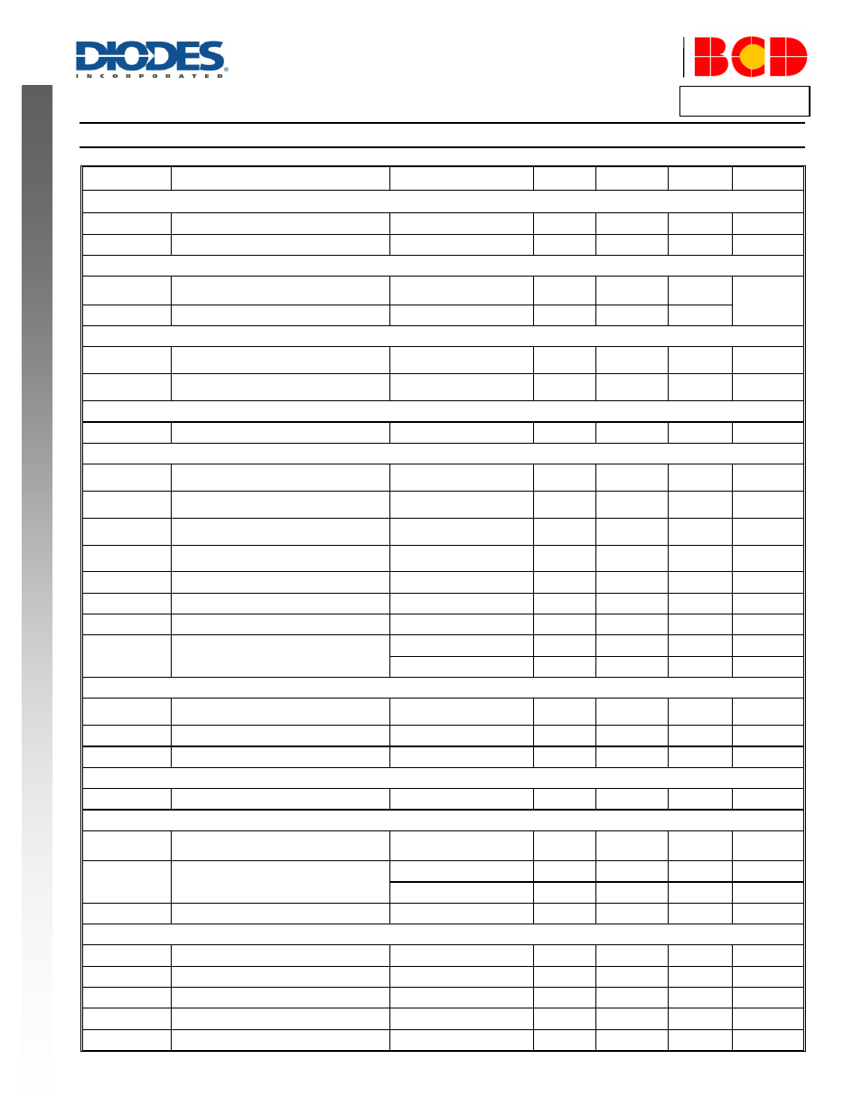
Electrical Characteristics
(@V
CC
=15V, T
J
=+25°C, unless otherwise specified.)
Symbol
Parameters
Conditions
Min
Typ
Max
Unit
STARTUP AND UVLO SECTION
V
TH_ST
Turn-on Voltage
–
13
15
17
V
V
OPR(MIN)
Turn-off Voltage
–
5.2
5.8
6.4
V
STANDBY CURRENT SECTION
I
ST
Turn-on Current
V
CC
=V
TH_ST
-1V before
startup
0
0.2
0.6
μA
I
CC_OPR
Operating Current
Static current @ no load
550
650
750
OPERATING FREQUENCY SECTION (5% LOAD TO FULL LOAD)
f
S(MAX)
Operating Frequency in Full Load
Condition
–
–
–
60
kHz
Δf/f
Frequency Dithering
5% to 100% of full load
range
4.5
5
5.5
%
OPERATING FREQUENCY SECTION (NO LOAD TO 5% OF I
OUT(MAX)
)
f
S(MIN)
Output Voltage Detection Frequency
–
1.8
2
2.2
kHz
CURRENT SENSE SECTION
V
CS_H
Peak Current Sense Voltage in Heavy
Load
40% to 100% of full load
874
910
946
mV
V
CS_M
Peak Current Sense Voltage in Middle
Load
18% to 40% of full load
581
605
630
mV
V
CS_L
Peak Current Sense Voltage in Light
Load
5% to 18% of full load
390
405
425
mV
V
CS_EL
Peak Current Sense Voltage in Extra-
Light Load
0% to 5% of full load
216
225
234
mV
ΔV
CS
/V
CS
V
CS
Modulation for Frequency Dithering
–
–
2.5
–
%
t
MOD
V
CS
Modulation Period
–
14.4
16
17.6
ms
R
LINE
Built-in Line Compensation Resistor
–
260
330
400
Ω
t
LEB
Leading Edge Blanking
@ V
CS_H
and
V
CS_M
410
500
575
ns
@ V
CS_EL
155
200
245
ns
CONSTANT VOLTAGE SECTION
V
FB
Equivalent Feedback Voltage @ Light
Load
Closed loop test of V
OUT
3.94
4.00
4.06
V
I
FB
FB Pin Input Current
V
FB
=4V
3.36
4.20
5.04
μA
V
CABLE
/V
OUT
Cable Compensation Ratio
(V
FB@FULLLOAD
-
V
FB
)
/
V
FB
5.65
6.00
6.40
%
CONSTANT CURRENT SECTION
t
ONS
/t
SW
Secondary Winding Conduction Duty
V
FB
=2V
–
4/7
–
–
POWER TRANSISTOR SECTION
V
CE(SAT)
Collector-emitter Saturation Voltage
AP3988/89: I
C
=0.5A
AP3990: I
C
=1A
–
–
0.3
V
h
FE
DC Current Gain
AP3988/89
14
17
–
–
AP3990
17
26
–
–
I
CEO
Leakage Current
–
–
–
60
μA
PROTECTION FUNCTION SECTION
V
FB(OVP)
Over Voltage Protection
–
–
7.5
–
V
V
FB(SCP)
Short Circuit Protection
V
FB
@ Hiccup
1.4
1.5
1.6
V
T
OTP
Shutdown Temperature
–
+125
+160
–
°C
T
HYS
Temperature Hysteresis
–
–
+40
–
°C
–
Driver Protection Voltage
–
4
5
6
V