Dq/dqs oct path, Dq/dqs oct path –14 – Altera ALTDLL User Manual
Page 50
Chapter 4: Functional Description
4–14
ALTDQ_DQS Megafunction
© February 2012
Altera Corporation
ALTDLL and ALTDQ_DQS Megafunctions User Guide
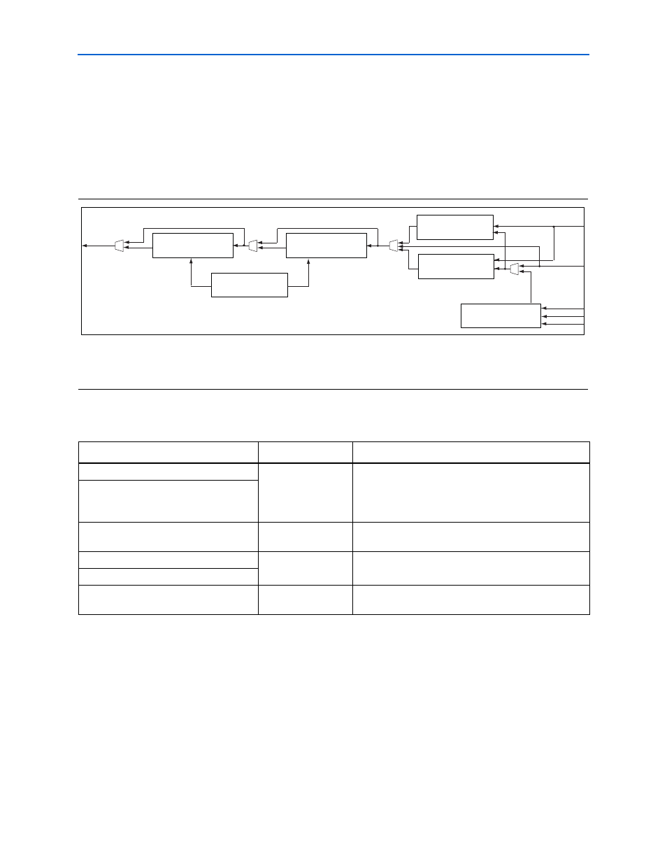
DQ/DQS OCT Path
shows the available blocks in the DQ/DQS OCT paths and the connections
with the ALTDQ_DQS ports. Use this path to utilize OCT capabilities at the DQ and
DQS output paths.
1
The <IO> value depends on your selection in the parameter editor. The possible
values are
DQS
,
DQSn
,
BIDIR_DQ
, and
OUTPUT_DQ
.
The DQ/DQS OCT path consists of the following blocks:
f
For more information about using the dynamic calibration blocks for termination,
refer to
.
For more information about implementing calibrated dynamic OCT, refer
Figure 4–7. DQ/DQS OCT Path
Notes to
(1) The <IO>
_oct_out
port must be connected to the input port of the output buffer.
(2) The <IO>
_OCT_HR_DDIO
block is a half-rate component.
<IO>_OCT_DELAY_CHAIN2 (D6 OCT)
DQS_CONFIG
<io>_oct_out
<IO>_OCT_DELAY_CHAIN1 (D5 OCT)
<IO>_OCT_FF
<IO>_OCT_DDIOE
<IO>_OCT_HR_DDIO
<io>_hr_oct_in[1]
<io>_hr_oct_in[0]
hr_oct_reg_clk
oct_reg_clk
<io>_oct_in
DQ/DQS OCT Path
Table 4–7. DQ/DQS OCT Path
Block
Name
Description
<IO>
_OCT_FF
OCT register blocks
The <IO>
_OCT_FF
block represents a group of flip-flop
registers in the DQ/DQS OCT output path.
The <IO>
_OCT_DDIOE
represents a group of DDIO
registers in the DQ/DQS OCT output path.
<IO>
_OCT_DDIOE
<IO>
_OCT_HR_DDIO
Half -rate OCT block
Represents a group of DDIO registers required to
transfer the calibrated output signal in half-rate mode.
<IO>
_OCT_DELAY_CHAIN1
(D5 OCT)
OCT delay chain
blocks
For more information about the OCT output delay chain
blocks, refer to
<IO>
_OCT_DELAY_CHAIN2
(D6 OCT)
DQS_CONFIG
DQS Configuration
Block
For more information about the
DQS_CONFIG
block,
refer to