Altera Phase-Locked Loop Reconfiguration IP Core User Manual
Page 30
Page 30
Design Example
Phase-Locked Loop Reconfiguration (ALTPLL_RECONFIG) Megafunction
February 2012
Altera Corporation
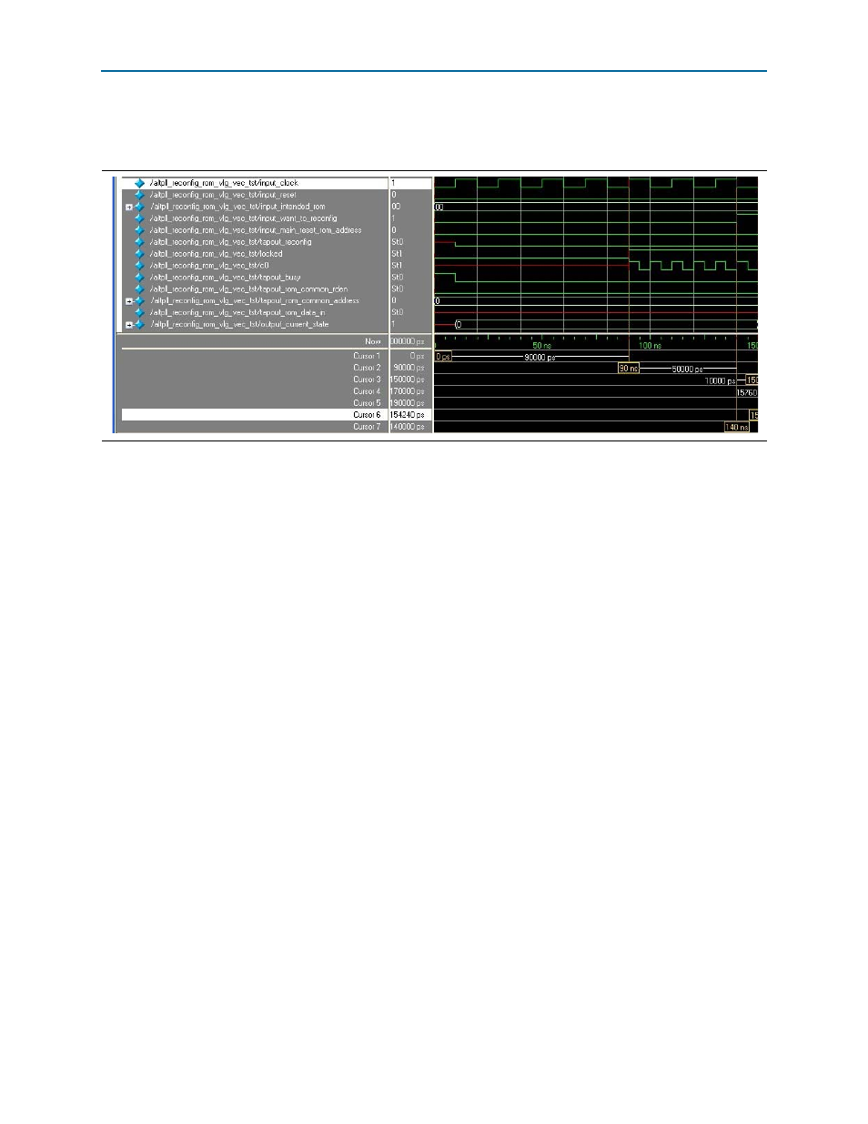
shows the simulation results when writing from ROM 1 to scan cache of the
ALTPLL_RECONFIG megafunction for the duration of 0 to 250 ns.
The simulation begins when the PLL gets locked (refer to
); the
locked
signal
is asserted at 90 ns. The PLL output
c0
produces a 100 MHz clock. The original
settings of the PLL have an input clock of 50 MHz and generates an output clock of
100 MHz.
1
The
output_current_state
signal is
0
, which shows the current state of the state
machine that controls the PLL reconfiguration process from the external ROMs.
When the state machine is at
0
(indicated by the output_current_state signal), it is
waiting for the assertion of the
input_want_to reconfig
signal together with the
value of the
input_intended_rom [1:0]
signal, which is
00
. The state machine
remains at this state until the above conditions are satisfied.
At 140 ns, the
input_want_to_reconfig
signal is asserted for 1 clock cycle and the
input_intended_rom [1:0]
signal is set to 00. The
input_want_to_reconfig
signal
controls the
write_from_rom
signal of the ALTPLL_RECONFIG instantiation. This
begins the process of writing the contents of the intended ROM to the scan cache of
the ALTPLL_RECONFIG megafunction. The
input_intended_rom [1:0]
signal is
used to control the selector (
sel
[1:0]
signal) of the multiplexer instantiation, which
multiplexes the intended ROM contents (in this case, ROM 1) to the
rom_data_in
signal of the ALTPLL_RECONFIG instantiation.
At 150 ns, the state machine is at
1
(indicated by the
output_current_state
signal).
This signifies that the
input_want_to_reconfig
signal has been asserted together with
the value of the
input_intended_rom [1:0]
signal, which is
00
. This causes the
write_from_rom
signal of the ALTPLL_RECONFIG instantiation to be asserted. This
also causes the selector (
sel [1:0]
signal) of the multiplexer instantiation to
multiplex the intended ROM contents (in this case, ROM 1) to the
rom_data_in
signal
of the ALTPLL_RECONFIG instantiation.
Figure 24. Initial Writing from ROM 1 to the Scan Cache of the ALTPLL_RECONFIG Megafunction (0 to 250 ns)