User-defined leds, General user-defined leds, User-defined leds –27 – Altera Stratix V Advanced Systems Development Board User Manual
Page 37: General user-defined leds –27
Chapter 2: Board Components
2–27
General User Input/Output
January 2014
Altera Corporation
Stratix V Advanced Systems Development Board
Reference Manual
User-Defined LEDs
The development board includes general, FMC, and HSMC user-defined LEDs. This
section describes all user-defined LEDs. For information on board specific or status
LEDs, refer to
“Status Elements” on page 2–18
.
General User-Defined LEDs
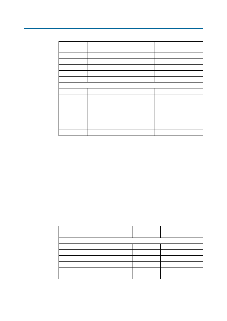
Board references D6 to D9, D17 to D20, D22 to D25, and D28 to D31 are two sets of
eight bi-color user LEDs which allow status and debugging signals to be driven to the
LEDs from the designs loaded into the Stratix V GX FPGA device. These LEDs are in
red and green, which combines to a total of 16 unique user LEDs. The LEDs illuminate
when a logic 0 is driven, and turns off when a logic 1 is driven. There is no board-
specific function for these LEDs.
Table 2–17
lists the user-defined LED schematic signal names and their corresponding
Stratix V GX FPGA pin numbers.
4
FPGA1_DIPSW3
1.5-V
AP24
5
FPGA1_DIPSW4
1.5-V
AP25
6
FPGA1_DIPSW5
1.5-V
AH27
7
FPGA1_DIPSW6
1.5-V
AN27
8
FPGA1_DIPSW7
1.5-V
BC29
FPGA2 User DIP Switch (SW3)
1
FPGA2_DIPSW0
1.5-V
T26
2
FPGA2_DIPSW1
1.5-V
V25
3
FPGA2_DIPSW2
1.5-V
H25
4
FPGA2_DIPSW3
1.5-V
P25
5
FPGA2_DIPSW4
1.5-V
G23
6
FPGA2_DIPSW5
1.5-V
C22
7
FPGA2_DIPSW6
1.5-V
H22
8
FPGA2_DIPSW7
1.5-V
T25
Table 2–16. User-Defined DIP Switch Schematic Signal Names and Functions (Part 2 of 2)
Board Reference
Schematic Signal Name
I/O Standard
Stratix V GX FPGA Device Pin
Number
Table 2–17. User-Defined LED Schematic Signal Names and Functions (Part 1 of 2)
Board Reference
Schematic Signal Name
I/O Standard
Stratix V GX FPGA Device
Pin Number
FPGA1 User LEDs
D20.3
FPGA1_LED_G0
1.5-V
H25
D20.4
FPGA1_LED_R0
1.5-V
N22
D19.3
FPGA1_LED_G1
1.5-V
P23
D19.4
FPGA1_LED_R1
1.5-V
P25
D18.3
FPGA1_LED_G2
1.5-V
AH19
D18.4
FPGA1_LED_R2
2.5-V
AR11