2 fpga jtag head, 3 switch settings, 1 pch switch – Artesyn ATCA 7370 / ATCA 7370-S Installation and Use (June 2014) User Manual
Page 74: Table 3-11, Switch sw2 settings, Figure 3-3, Usb 2.0 flash disk module connector pinout
Advertising
Controls, Indicators, and Connectors
ATCA-7370/ATCA-7370-S Installation and Use (6806800P54F)
74
3.2.4.2
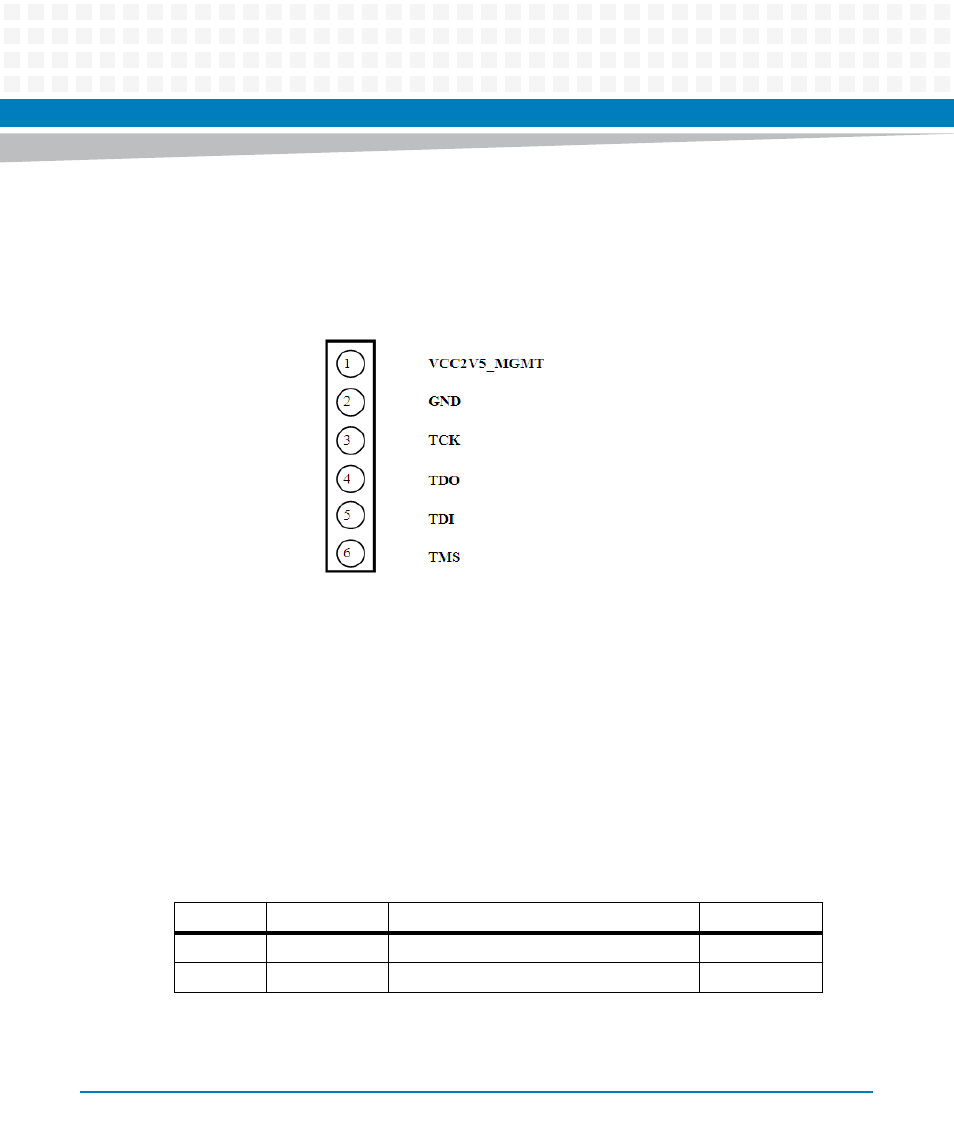
FPGA JTAG Head
A single row six-pin heads for FPGA programming through JTAG is provided on the board.
3.3
Switch Settings
Switches reside on the component side 1 of the board and are not covered by any other
component. Its pin 1 is clearly marked on the PCB and by default are "OFF".
3.3.1
PCH Switch
Figure 3-3
USB 2.0 Flash Disk Module Connector Pinout
Table 3-11 Switch SW2 Settings
Switch
PCH
Function
Default
SW2.1
GPIO6
ON: Load default BIOS setting
OFF
SW2.2
GPIO7
ON: BIOS Crisis Recovery
OFF
Advertising
This manual is related to the following products: